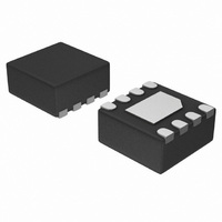
NCP5359AMNR2G ON Semiconductor, NCP5359AMNR2G Datasheet - Page 4

NCP5359AMNR2G
Manufacturer Part Number
NCP5359AMNR2G
Description
IC MOSFET GATE DVR DUAL 8-DFN
Manufacturer
ON Semiconductor
Type
High Side/Low Sider
Datasheet
1.NCP5359AMNTBG.pdf
(9 pages)
Specifications of NCP5359AMNR2G
Configuration
High and Low Side, Synchronous
Input Type
PWM
Delay Time
10.0ns
Number Of Configurations
1
Number Of Outputs
2
High Side Voltage - Max (bootstrap)
30V
Voltage - Supply
10 V ~ 13.2 V
Operating Temperature
0°C ~ 85°C
Mounting Type
Surface Mount
Package / Case
8-VFDFN Exposed Pad
Product
MOSFET Gate Drivers
Propagation Delay Time
25 ns
Supply Voltage (max)
15 V
Supply Voltage (min)
- 0.3 V
Maximum Operating Temperature
+ 150 C
Mounting Style
SMD/SMT
Minimum Operating Temperature
0 C
Output Voltage
35 V
Lead Free Status / RoHS Status
Lead free / RoHS Compliant
Current - Peak
-
Lead Free Status / Rohs Status
Lead free / RoHS Compliant
Available stocks
Company
Part Number
Manufacturer
Quantity
Price
Company:
Part Number:
NCP5359AMNR2G
Manufacturer:
FREESCALE
Quantity:
101
Part Number:
NCP5359AMNR2G
Manufacturer:
ON/安森美
Quantity:
20 000
Stresses exceeding Maximum Ratings may damage the device. Maximum Ratings are stress ratings only. Functional operation above the
Recommended Operating Conditions is not implied. Extended exposure to stresses above the Recommended Operating Conditions may affect
device reliability.
1. Latchup Current Maximum Rating: 100 mA per JEDEC standard: JESD78.
2. Moisture Sensitivity Level (MSL): 1&3 per IPC/JEDEC standard: J−STD−020A.
3. The maximum package power dissipation limit must not be exceeded.
NOTE:
MAXIMUM RATINGS
Thermal Characteristics, Plastic Package
Thermal Resistance Junction−to−Air
Operating Junction Temperature Range
Operating Ambient Temperature Range
Storage Temperature Range
Moisture Sensitivity Level
MAXIMUM RATINGS
PD +
Pin Symbol
This device is ESD sensitive. Use standard ESD precautions when handling.
DRVH
DRVL
PWM
GND
BST
Vcc
SW
EN
TJ(max) * TA
RqJA
Rating
DRVH and DRVL Control Input
Main Supply Voltage Input
(Bootstrap Supply Return)
Bootstrap Supply voltage
High Side Driver Output
Low Side Driver Output
Switching Node
Enable Pin
Pin Name
Ground
(20.2 sq mm, 2 oz Cu) DFN8
http://onsemi.com
4
SOIC−8
SOIC−8
DFN8
40 V ≤ 50 ns wrt / GND
40 V ≤ 50 ns wrt / GND
35 V ≤ 50 ns wrt / GND
Symbol
R
35 V wrt / GND
35 V wrt / GND
MSL
T
15 V wrt / SW
15 V wrt / SW
T
T
BST + 0.3 V
qJA
stg
Vcc + 0.3 V
A
J
V
15 V
6 V
6 V
0 V
MAX
− 55 to +150
0 to +150
0 to +85
Value
178
330
−2 V (200 ns) wrt / SW
1
1
−0.3 V wrt / SW
−0.3 V wrt / SW
−10 V (200 ns)
−5 V (200 ns)
−1 VDC
−0.3 V
−0.3 V
−0.3 V
−0.3 V
V
0 V
MIN
°C/W
Unit
°C
°C
°C
−


