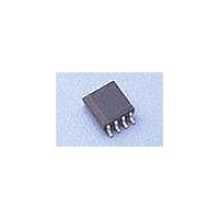
TC427EUA713 Microchip Technology, TC427EUA713 Datasheet - Page 6

TC427EUA713
Manufacturer Part Number
TC427EUA713
Description
IC MOSFET DVR 1.5A DUAL HS 8MSOP
Manufacturer
Microchip Technology
Type
Microcontrollerr
Datasheet
1.TC427EOA.pdf
(16 pages)
Specifications of TC427EUA713
Configuration
Low-Side
Input Type
Non-Inverting
Delay Time
50ns
Current - Peak
1.5A
Number Of Configurations
2
Number Of Outputs
2
Voltage - Supply
4.5 V ~ 18 V
Operating Temperature
-40°C ~ 85°C
Mounting Type
Surface Mount
Package / Case
8-TSSOP, 8-MSOP (0.118", 3.00mm Width)
Rise Time
30 ns
Fall Time
30 ns
Supply Voltage (min)
4.5 V
Supply Current
8 mA
Maximum Power Dissipation
340 mW
Maximum Operating Temperature
+ 85 C
Mounting Style
SMD/SMT
Minimum Operating Temperature
- 40 C
Number Of Drivers
2
Lead Free Status / RoHS Status
Lead free / RoHS Compliant
High Side Voltage - Max (bootstrap)
-
Lead Free Status / Rohs Status
Lead free / RoHS Compliant
TC426/TC427/TC428
3.0
3.1
Charging and discharging large capacitive loads
quickly requires large currents. For example, charging
a 1000pF load to 18V in 25nsec requires an 0.72A
current from the device power supply.
To ensure low supply impedance over a wide frequency
range, a parallel capacitor combination is recom-
mended for supply bypassing. Low-inductance ceramic
disk capacitors with short lead lengths (< 0.5 in.) should
be used. A 1µF film capacitor in parallel with one or two
0.1µF ceramic disk capacitors normally provides
adequate bypassing.
3.2
The TC426 and TC428 contain inverting drivers.
Ground potential drops developed in common ground
impedances from input to output will appear as
negative feedback and degrade switching speed
characteristics.
Individual ground returns for the input and output
circuits or a ground plane should be used.
3.3
The input voltage level changes the no-load or
quiescent supply current. The N-channel MOSFET
input stage transistor drives a 2.5mA current source
load. With a logic "1" input, the maximum quiescent
supply current is 8mA. Logic "0" input level signals
reduce quiescent
Minimum power dissipation occurs for logic "0" inputs
for the TC426/TC427/TC428. Unused driver inputs
must be connected to V
The drivers are designed with 100mV of hysteresis.
This provides clean transitions and minimizes output
stage current spiking when changing states. Input
voltage thresholds are approximately 1.5V, making the
device TTL compatible over the 4.5V to 18V supply
operating range. Input current is less than 1µA over this
range.
The TC426/TC427/TC428 may be directly driven by
the TL494, SG1526/1527, SG1524, SE5560, and
similar switch-mode power supply integrated circuits.
DS21415B-page 6
APPLICATIONS INFORMATION
Supply Bypassing
Grounding
Input Stage
current to 0.4mA maximum.
DD
or GND.
3.4
The supply current vs frequency and supply current
vs capacitive load characteristic curves will aid in
determining power dissipation calculations.
The TC426/TC427/TC428 CMOS drivers have greatly
reduced quiescent DC power consumption. Maximum
quiescent current is 8mA compared to the DS0026
40mA specification. For a 15V supply, power
dissipation is typically 40mW.
Two other power dissipation components are:
• Output stage AC and DC load power.
• Transition state power.
Output stage power is:
Where:
In power MOSFET drive applications the P
negligible. MOSFET power transistors are high imped-
ance, capacitive input devices. In applications where
resistive loads or relays are driven, the P
will normally dominate.
The magnitude of P
cases:
During output level state changes, a current surge will
flow through the series connected N and P channel
output MOSFETS as one device is turning "ON" while
the other is turning "OFF". The current spike flows only
during output transitions. The input levels should not be
maintained between the logic "0" and logic "1" levels.
Unused driver inputs must be tied to ground and
not be allowed to float. Average power dissipation will
be reduced by minimizing input rise times. As shown in
the characteristic curves, average supply current is
frequency dependent.
A.
Po = P
Vo = DC output voltage
I
f
Vs = Supply voltage
DC
1. f
2. C
3. Vs = 18V
4. P
= Vo (I
= DC output load current
= Switching frequency
Power Dissipation
AC
L
DC
= 200kHZ
=1000pf
= 65mW
DC
+ PAC
) + f C
AC
is readily estimated for several
2002 Microchip Technology Inc.
L
V
S
2
B.
1. f
2. C
3. Vs = 15V
4. P
AC
L
= 200kHz
=1000pf
= 45mW
DC
component
DC
term is


