IR3839MTRPBF International Rectifier, IR3839MTRPBF Datasheet
IR3839MTRPBF
Specifications of IR3839MTRPBF
Available stocks


Related parts for IR3839MTRPBF


IR3839MTRPBF Summary of contents
Page 1
SupIRBuck TM SINGLE-INPUT VOLTAGE, SYNCHRONOUS BUCK REGULATOR Features • Greater than 96% Maximum Efficiency • Single 16V Application • Single 5V Application • Wide Output Voltage Range: 0.6V to 0.9*Vin • Continuous 6A Load Capability • Programmable Switching Frequency up ...
Page 2
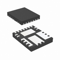
... Power QFN (Top View) Boot Enable Vp ORDERING INFORMATION PACKAGE DESIGNATOR M M Rev 1 PGnd SW PVin Gnd Vref Comp Gnd Rt OCset PGood PACKAGE PIN COUNT DESCRIPTION IR3839MTRPbF 17 IR3839MTR1PbF 17 IR3839MPbF o C and - θ θ PCB Vcc/LDO_out Vin Sync PARTS PER REEL 4000 750 2 ...
Page 3
Block Diagram V LDO_Ref LDO Gnd + - Comp VREF Vref Vp Fb Intl_SS SOFT FAULT START SSOK POR VREF UVEN UVEN Enable POR UVcc Rev 1.2 Vin Vcc/LDO_out UVcc UVcc VCC POR FAULT CONTROL POR 0.6V + E/A + ...
Page 4
Pin Description Pin Name Description Inverting input to the error amplifier. This pin is connected directly to the 1 Fb output of the regulator via resistor divider to set the output voltage and provide feedback to the error amplifier External ...
Page 5
Recommended Operating Conditions Symbol Definition PVin Input Voltage for power stage Vin Input Voltage for internal LDO * Vcc/LDO_out Supply Voltage * Boot to SW Supply Voltage V Output Voltage o I Output Current o Fs Switching Frequency T Junction ...
Page 6
Electrical Specifications (continued) Unless otherwise specified, these specification apply over, 7.0V< C<T < 125 o C. Typical values are specified PARAMETER ERROR AMPLIFIER Input Offset Voltage Input Bias Current Input Bias Current Sink Current ...
Page 7
Electrical Specifications (continued) PARAMETER FAULT PROTECTION OCSET Current OC comp Offset Voltage SS off time Thermal Shutdown Thermal Hysteresis UNDER VOLTAGE LOCKOUT V -Start-Threshold -Stop-Threshold Enable-Start-Threshold Enable_UVLO_Start Enable-Stop-Threshold Enable_UVLO_Stop Enable leakage current PGOOD ...
Page 8
Typical Efficiency and Power Loss Curves Vin=12V, Vcc=5V (external), Io=0.5A-6A, F The table below shows the inductors used for each of the output voltages in the efficiency measurement. Vo [V] L [µH] 1.2 1.8 3.3 5 ...
Page 9
Typical Efficiency and Power Loss Curves Vin=12V, Vcc/LDO_out=5.2V, Io=0.5A-6A, Fs=600kHz, Room Temperature, No Air Flow The same inductors as listed on the previous page have been used 0.5 ...
Page 10
TYPICAL OPERATING CHARACTERISTICS (-40 Iin(Standby) 400 380 360 340 320 300 280 260 240 220 200 180 160 -40 - Temp [ºC] FREQUENCY 550 540 530 520 510 500 490 480 470 460 450 -40 -20 ...
Page 11
Rdson of MOSFETs Over Temperature at Vcc= -40 -20 0 Rdson of Sync-FET versus Vcc at different Temperatures 4.5 4.75 -40C Rev 1 ...
Page 12
Circuit Description THEORY OF OPERATION Introduction The IR3839 uses a PWM voltage mode control scheme with external compensation to provide good noise immunity and maximum flexibility in selecting inductor values and capacitor types. The switching frequency is programmable from 250kHz ...
Page 13
Fig. 4a. Recommended startup for Normal operation Pvin (12V) Vcc (5.2V) Fig. 4b. Recommended startup for sequencing operation (ratiometric or simultaneous) Fig. 4c. Recommended startup for memory tracking operation (Vtt-DDR) Rev 1.2 Vref This pin reflects the internal reference voltage ...
Page 14
Soft-Start The IR3839 has a digital internal soft-start to control the output voltage rise and to limit the current surge at the start-up. To ensure correct start-up, the soft-start sequence initiates when the Enable and Vcc rise above their UVLO ...
Page 15
Fig. 7. Connection of over current sensing resistor As mentioned earlier, an over current is detected if the OCSet pin goes below ground. Hence, at the current limit threshold, V OCset current limit setting Limit OCSet follows: ...
Page 16
Therefore, in normal operating condition, after Enable goes high the SS ramps up the output voltage until Vfb (voltage of feedback/Fb pin) reaches about 0.6V. Then Vref takes over and the output voltage is regulated (refer to Fig. 11). Tracking-mode ...
Page 17
Power Good Output The IC continually monitors the output voltage via Feedback (Fb pin). The feedback voltage is compared to a threshold. The threshold is set differently at different operating modes and the results of the comparison sets the PGood ...
Page 18
TIMING DIAGRAM OF PGOOD FUNCTIONS Fig.12 Vp Tracking (Vref >1.5V, SS=H) Fig.13 Vp Sequence and Vref Margin Rev 1.2 IR3839MPbF 18 ...
Page 19
Minimum on time Considerations The minimum ON time is the shortest amount of time for which the Control FET may be reliably turned on, and this depends on the internal timing delays. For the IR3839, the typical minimum on-time is ...
Page 20
Application Information Design Example: The following example is a typical application for IR3839. The application circuit is shown on page 26 max ...
Page 21
Fig. 17. Bootstrap circuit to generate Vc voltage A bootstrap capacitor of value 0.1uF is suitable for most applications. Input Capacitor Selection The ripple current generated during the on time of the control FET should be provided by the input ...
Page 22
Where: ∆V = output voltage ripple o ∆I = Inductor ripple current L Since the output capacitor has a major role in the overall performance of the determines the result of transient response, selection of the capacitor is critical. The ...
Page 23
The transfer function ( given by: e out Z out IN 8 The (s) indicates that the ...
Page 24
Again, the transfer function is given by out IN By replacing Z and Z according to figure 20 the transfer function can be expressed as: ...
Page 25
Select crossover frequency F =100 kHz 0 Since F <F <Fs/2<F , Type III is selected ESR place the pole and zeros. Detailed calculation of compensation Type III : Desired Phase Margin 1 ...
Page 26
... Panasonic - ECG Thick Film, 0603,1/10W,1% Rohm Thick Film, 0603,1/10W,1% Rohm Thick Film, 0603,1/10W,1% Panasonic - ECG 0603, 50V, X7R, 10% Panasonic - ECG 0603, 10V, X5R, 10% Panasonic - ECG SupIRBuck, 6A, PQFN 5x6mm International Rectifier IR3839MPbF Part Number EEV-FK1E331P ECJ-3YX1C106K SPM6550T-1R0M100A C2012X5R0J226M MCR03EZPFX4992 MCR03EZPFX6801 MCR03EZPFX2372 MCR03EZPFX5901 MCR03EZPFX1002 ...
Page 27
TYPICAL OPERATING WAVEFORMS Vin=12V, Vcc/LDO=5.2V, Vo=1.8V, Io=0-6A, Room Temperature, No Air Flow Fig. 22: Start Load (Note :PGood Ch : out 2 3 Fig. 24: Start up with 1.62V Prebias, 0A ...
Page 28
TYPICAL OPERATING WAVEFORMS Vin=12V, Vcc/LDO=5.2V, Vo=1.8V, Room Temperature, No Air Flow 2.4A(40%)-4.2A(70%) load (0.5A/us) Ch Note5: Enable (EN) is tied to Vin via a resistor divider and triggered when Vin is exceeding above 10.2V. Rev 1.2 Fig. 28: Transient Response ...
Page 29
TYPICAL OPERATING WAVEFORMS Vin=12V, Vcc/LDO=5.2V, Vo=1.8V, Io=0-6A, Room Temperature, No Air Flow Fig.29: Bode Plot at 6A load shows a bandwidth of 104kHz and phase margin of 51 degrees Rev 1.2 IR3839MPbF 29 ...
Page 30
Layout Considerations The layout is very important when designing high frequency switching converters. Layout will affect noise pickup and can cause a good design to perform with less than expected results. Make all the connections components in the top layer ...
Page 31
Boot cap uses separate trace from OCSet connected to SW node Fig. 30b. IRDC3839 demoboard layout considerations – Bottom Layer Analog Ground plane Single point connection between AGND & PGND, should be close to the SupIRBuck, kept ...
Page 32
PCB Metal and Components Placement The lead lands (the 13 IC pins) width should be equal to the nominal part lead width. The minimum lead to lead spacing should be ≥ 0.2mm to minimize shorting. Lead land length should be ...
Page 33
Solder Resist It is recommended that the lead lands are Non Solder Mask Defined (NSMD). The solder resist should be pulled away from the metal lead lands by a minimum of 0.025mm to ensure NSMD pads. The land pad should ...
Page 34
Stencil Design • The Stencil apertures for the lead lands should be approximately 80% of the area of the lead lads. Reducing the amount of solder deposited will minimize the occurrences of lead shorts. If too much solder is deposited ...
Page 35
MILIMITERS INCHES DIM MIN MAX MIN A 0.800 1.000 0.0315 A1 0.000 0.050 0.0000 b 0.375 0.475 0.1477 b1 0.250 0.350 0.0098 c 0.203 REF. 0.008 REF. D 5.000 BASIC 1.969 BASIC E 6.000 BASIC 2.362 BASIC e 1.033 BASIC ...