CP2501DK Silicon Laboratories Inc, CP2501DK Datasheet - Page 8
CP2501DK
Manufacturer Part Number
CP2501DK
Description
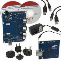
KIT DEVELOPMENT CP2501
Manufacturer
Silicon Laboratories Inc
Datasheets
1.CP2501DK.pdf
(14 pages)
2.CP2501DK.pdf
(2 pages)
3.CP2501DK.pdf
(2 pages)
4.CP2501DK.pdf
(30 pages)
5.CP2501DK.pdf
(1 pages)
6.CP2501DK.pdf
(2 pages)
Specifications of CP2501DK
Main Purpose
Interface, Touch Screen Controller
Embedded
Yes, MCU, 8-Bit
Utilized Ic / Part
CP2501
Primary Attributes
USB Configurable Parameters such as VID, PID and Strings
Secondary Attributes
GPIO, I²:C; SMBus, SPI, UART Interface
Interface Type
USB, I2C, SPI, UART
Operating Voltage
3.3 V
Data Bus Width
16 bit
Maximum Operating Temperature
+ 85 C
Minimum Operating Temperature
- 40 C
For Use With/related Products
CP2501
Lead Free Status / RoHS Status
Lead free / RoHS Compliant
Other names
336-1988


CP2501-DK
5.1. Switch and LEDs
The RESET switch is connected to the RST pin of the CP250x. Pressing RESET puts the device into its hardware-
reset state.
Four LEDs are also provided on the motherboard. The red LED labeled “PWR” (D4), indicates a power connection
to the motherboard. The green LED labeled “RUN” (D10) turns on when the debug circuitry is in a running state;
the red LED labeled “STOP” (D11) turns on when the debug circuitry is in a halted state, and the orange LED
labeled “DEBUG PWR” (D12) indicates whether the debug adapter circuit is being powered through P5's USB
connector. Table 2 lists the port pins and headers corresponding to the switch and LEDs.
5.2. Power Supply Headers (P3, J3, and J7)
The main power supply of the motherboard, which is used to power the daughter board, can be provided by either
the USB debug device’s on-chip voltage regulator or P3 and its associated circuitry. To select a power supply, place
a shorting block on J3 across the appropriate pin pair, as shown in Figure 5. To connect the main power supply to
an attached daughter board, place a shorting block across J7.
Notes:
8
Orange LED labeled "DEBUG PWR"
1. Only two of the pins on the J3 header should be connected at any one time
2.
To use the USB debug device’s voltage regulator as the board's power supply, a USB cable must be
connected to P5, and the DEBUG PWR LED (D12) must be on.
Green LED labeled "RUN"
Red LED labeled "STOP"
Red LED labeled "PWR"
Description
RESET
Figure 5. J3 and J7 Shorting Block Configuration for Power Options
J7
VDD_CP250x
Table 2. Motherboard LED and Switch Descriptions
+3.3V Regulator Power
VDD_PWR
(From P3)
J3
VDD_DEBUG
VDD_PWR
+3VD
Component Name
SW3
D10
D12
D11
D4
Rev. 0.1
VDD_CP250x
J7
VDD_PWR
Daughter Board’s RST/C2CK
Debug Circuit Power
(From USB at P5)
Daughter Board’s VDD
Debug Adapter Signal
Debug Adapter Signal
Debug Adapter Signal
J3
VDD_DEBUG
VDD_PWR
+3VD
I/O
Header
J3, J7
None
None
None
None
Related parts for CP2501DK
Image
Part Number
Description
Manufacturer
Datasheet
Request
R

Part Number:
Description:
IC TOUCH SCREEN USB BRIDGE 32QFN
Manufacturer:
Silicon Laboratories Inc
Datasheet:
Part Number:
Description:
Microcontrollers (MCU) Touch screen USB Bridge
Manufacturer:
Silicon Laboratories Inc
Part Number:
Description:
SMD/C°/SINGLE-ENDED OUTPUT SILICON OSCILLATOR
Manufacturer:
Silicon Laboratories Inc
Part Number:
Description:
Manufacturer:
Silicon Laboratories Inc
Datasheet:
Part Number:
Description:
N/A N/A/SI4010 AES KEYFOB DEMO WITH LCD RX
Manufacturer:
Silicon Laboratories Inc
Datasheet:
Part Number:
Description:
N/A N/A/SI4010 SIMPLIFIED KEY FOB DEMO WITH LED RX
Manufacturer:
Silicon Laboratories Inc
Datasheet:
Part Number:
Description:
N/A/-40 TO 85 OC/EZLINK MODULE; F930/4432 HIGH BAND (REV E/B1)
Manufacturer:
Silicon Laboratories Inc
Part Number:
Description:
EZLink Module; F930/4432 Low Band (rev e/B1)
Manufacturer:
Silicon Laboratories Inc
Part Number:
Description:
I°/4460 10 DBM RADIO TEST CARD 434 MHZ
Manufacturer:
Silicon Laboratories Inc
Part Number:
Description:
I°/4461 14 DBM RADIO TEST CARD 868 MHZ
Manufacturer:
Silicon Laboratories Inc
Part Number:
Description:
I°/4463 20 DBM RFSWITCH RADIO TEST CARD 460 MHZ
Manufacturer:
Silicon Laboratories Inc
Part Number:
Description:
I°/4463 20 DBM RADIO TEST CARD 868 MHZ
Manufacturer:
Silicon Laboratories Inc
Part Number:
Description:
I°/4463 27 DBM RADIO TEST CARD 868 MHZ
Manufacturer:
Silicon Laboratories Inc
Part Number:
Description:
I°/4463 SKYWORKS 30 DBM RADIO TEST CARD 915 MHZ
Manufacturer:
Silicon Laboratories Inc