RMPA1959 Fairchild Semiconductor, RMPA1959 Datasheet - Page 2
RMPA1959
Manufacturer Part Number
RMPA1959
Description
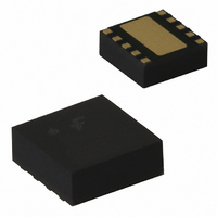
IC MOD RF POWER AMP 10PIN 4X4LCC
Manufacturer
Fairchild Semiconductor
Type
Power Amplifierr
Datasheet
1.RMPA1959.pdf
(11 pages)
Specifications of RMPA1959
Current - Supply
50mA
Frequency
1.85GHz ~ 1.91GHz
Gain
23dB ~ 25dB
Noise Figure
4dB
Package / Case
11-LCC
Rf Type
CDMA, CDMA2000, PCS
Voltage - Supply
3V ~ 4.2V
Number Of Channels
1
Frequency (max)
1.91GHz
Output Power
28@1880MHzdBm
Power Supply Requirement
Single
Single Supply Voltage (min)
3V
Single Supply Voltage (typ)
3.4V
Single Supply Voltage (max)
4.2V
Package Type
PLCC
Dual Supply Voltage (min)
Not RequiredV
Dual Supply Voltage (typ)
Not RequiredV
Dual Supply Voltage (max)
Not RequiredV
Operating Temperature Classification
Commercial
Operating Temp Range
-30C to 85C
Pin Count
10
Mounting
Surface Mount
Lead Free Status / RoHS Status
Lead free / RoHS Compliant
P1db
-
Test Frequency
-
Lead Free Status / Rohs Status
Compliant
Other names
RMPA1959TR
Available stocks
Company
Part Number
Manufacturer
Quantity
Price
Company:

Part Number:
RMPA1959
Manufacturer:
Fairchild
Quantity:
25


©2004 Fairchild Semiconductor Corporation
Module Block Diagram
Electrical Characteristics
Notes:
1: All parameters met at Tc = +25°C, Vcc = +3.4V, f = 1880 MHz, and load VSWR ≤ 1.2:1.
2: All phase angles.
3: Guaranteed by design
CDMA Operation
General Characteristics
DC Characteristics
Symbol
Icc (off)
ACPR1
ACPR2
VSWR
2fo-5fo
Rx No
PAEd
SSg
Iccq
Iref
Gp
Itot
NF
P
Tc
S
f
O
Figure 1. RMPA1959 US PCS CDMA Power Amplifier Module Functional Block Diagram
VCC1, VCC2
Operating Frequency
Small-Signal Gain
Power Gain
Linear Output Power
PAEd (digital) @ +28 dBm
PAEd (digital) @ +16 dBm
PAEd (digital) @ +16 dBm
High Power Total Current
Low Power Total Current
Adjacent Channel Power Ratio
±1.25 MHz Offset
±2.25 MHz Offset
Input Impedance
Noise Figure
Receive Band Noise Power
Harmonic Suppression
Spurious Outputs
Ruggedness w/Load Mismatch
Case Operating Temperature
Quiescent Current
Reference Current
Leakage Shutdown Current
(1, 10)
VREF
RF IN
(2)
(5)
Parameter
MATCHING
NETWORK
INPUT
2,3
1
INPUT STAGE
3
P
P
P
Vmode = 0V
Vmode ≥ 2.0V
Vmode = 0V
Vmode ≥ 2.0V
Vmode ≥ 2.0V, V
P
P
IS-95
P
P
P
P
P
P
Load VSWR ≤ 5.0:1
No permanent damage
Vmode ≥ 2.0V
P
No applied RF signal
BIAS
O
O
O
O
O
O
O
O
O
O
O
O
INPUT
STAGE
= 0dBm
= +28dBm, Vmode = 0V
= +16dBm, Vmode ≥ 2.0V
= +28dBm, Vmode = 0V
= +16dBm, Vmode = 2.0V
= +28dBm; Vmode = 0V
= +16dBm; Vmode = 2.0V
= +28dBm; Vmode = 0V
= +16dBm; Vmode = 2.0V
≤ +28dBm; 1850 to 1910 MHz
≤ +28dBm
≤ +28dBm
Vmode (4)
COLLECTOR
INTERSTAGE
CONTROL
MMIC
BIAS
MATCH
BIAS
Condition
CC
OUTPUT STAGE
= 1.4V
BIAS
OUTPUT
STAGE
PA MODULE
MATCHING
NETWORK
OUTPUT
1850
2.5:1
Min
-30
23
25
28
36
VCC=3.4V (nom)
VREF=2.85V (nom)
1850–1910 MHz
50 Ohms I/O
RF OUT
(8)
GND
(3, 6, 7, 9, 11)
2.0:1
24.5
-139
Typ
460
120
-50
-52
-60
-68
25
28
39
10
20
50
4
5
1
1910
Max
10:1
530
-46
-57
-30
-60
16
85
8
5
RMPA1959 Rev. D
dBm/Hz
Units
MHz
dBm
dBm
dBc
dBc
dBc
dBc
dBc
dBc
mA
mA
mA
mA
dB
dB
dB
dB
°C
µA
%
%
%
Related parts for RMPA1959
Image
Part Number
Description
Manufacturer
Datasheet
Request
R

Part Number:
Description:
Fairchild Semiconductor [IGBT MODULE]
Manufacturer:
Fairchild Semiconductor
Datasheet:

Part Number:
Description:
Discrete Semiconductor Modules
Manufacturer:
Fairchild Semiconductor
Part Number:
Description:
Discrete Semiconductor Modules
Manufacturer:
Fairchild Semiconductor
Part Number:
Description:
This N-Channel MOSFET is produced using Fairchild Semiconductor’s advanced Power Trench® process
Manufacturer:
Fairchild Semiconductor
Datasheet:
Part Number:
Description:
This N-Channel MOSFET is produced using Fairchild Semiconductor’s advanced Power Trench® process
Manufacturer:
Fairchild Semiconductor
Datasheet:
Part Number:
Description:
This N-Channel MOSFET is produced using Fairchild Semiconductor’s advanced PowerTrench® process
Manufacturer:
Fairchild Semiconductor
Datasheet:
Part Number:
Description:
This N-Channel MOSFET is produced using Fairchild Semiconductor’s advanced PowerTrench® process
Manufacturer:
Fairchild Semiconductor
Datasheet:
Part Number:
Description:
This N-Channel MOSFET is produced using Fairchild Semiconductor’s advanced Power Trench® process
Manufacturer:
Fairchild Semiconductor
Datasheet:
Part Number:
Description:
This N-Channel logic Level MOSFETs are produced using Fairchild Semiconductor‘s advanced Power Trench® process that has been special tailored to minimize the on-state resistance and yet maintain superior switching performance
Manufacturer:
Fairchild Semiconductor
Datasheet:
Part Number:
Description:
This N-Channel MOSFET is produced using Fairchild Semiconductor’s advanced Power Trench® process
Manufacturer:
Fairchild Semiconductor
Datasheet:
Part Number:
Description:
This N-Channel SyncFET™ is produced using Fairchild Semiconductor’s advanced PowerTrench® process
Manufacturer:
Fairchild Semiconductor
Datasheet:
Part Number:
Description:
This N-Channel SyncFET™ is produced using Fairchild Semiconductor’s advanced PowerTrench® process
Manufacturer:
Fairchild Semiconductor
Datasheet:
Part Number:
Description:
This N-Channel SyncFET™ is produced using Fairchild Semiconductor’s advanced PowerTrench® process
Manufacturer:
Fairchild Semiconductor
Datasheet:
Part Number:
Description:
This N-Channel logic Level MOSFETs are produced using Fairchild Semiconductor‘s advanced Power Trench® process that has been special tailored to minimize the on-state resistance and yet maintain superior switching performance
Manufacturer:
Fairchild Semiconductor
Datasheet:
Part Number:
Description:
This N-Channel MOSFET is produced using Fairchild Semiconductor’s advanced Power Trench® process that has been especially tailored to minimize the on-state resistance and yet maintain superior switching performance
Manufacturer:
Fairchild Semiconductor
Datasheet: