SKY65116-21 Skyworks Solutions Inc, SKY65116-21 Datasheet - Page 9
SKY65116-21
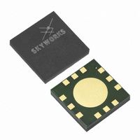
Manufacturer Part Number
SKY65116-21
Description
IC AMP LINEAR 390-500MHZ 12-MCM
Manufacturer
Skyworks Solutions Inc
Datasheet
1.SKY65116-21.pdf
(14 pages)
Specifications of SKY65116-21
Current - Supply
1.3A
Frequency
390MHz ~ 500MHz
Gain
35dB
Noise Figure
6dB
P1db
32.5dBm
Package / Case
12-MCM
Rf Type
GSM, NMT, TETRA, UHF, WLL
Voltage - Supply
4.5V
Lead Free Status / RoHS Status
Lead free / RoHS Compliant
Test Frequency
-
Other names
863-1072-2
Available stocks
Company
Part Number
Manufacturer
Quantity
Price
Company:

Part Number:
SKY65116-21
Manufacturer:
TI
Quantity:
14 300


Theory of Operation
The SKY65116 is comprised of two amplifier stages, and is
internally matched for optimum linearity and efficiency. The
matching circuits for the input stage, inter-stage, and output stage
are contained within the device. An on-chip active bias circuit is
included within the device for both input and output stages pro-
viding for excellent gain tracking over temperature and voltage
variations. The module operates with all positive DC voltages
while maintaining high efficiency and good linearity. The nominal
operating voltage is 3.6 V for maximum power, but can be oper-
ated at slightly lower voltages for other mobile applications.
The input and output stages are independently supplied using the
V
reference voltage is supplied using a common V
The module includes a silicon CMOS controller circuit to
provide an amplifier On/Off operation. V
off control voltage to the CMOS controller for stages 1 and 2. 0 V
= Off, 3.6 V = On. Nominal “On” operating range is between 2.7
to 3.6 V
off mode, drawing only microamperes of current.
Application Circuit Notes
Center Ground. It is extremely important that the device paddle
be sufficiently grounded for both thermal and stability reasons.
Multiple small vias are acceptable and will work well under the
device if solder migration is an issue.
Ground (Pins 1, 3, 5, 6, 7, 9). Attach all ground pins to the RF
ground plane with the largest diameter and lowest inductance
via that the layout will allow. Multiple small vias are also
acceptable and will work well under the device if solder
migration is an issue.
RF_IN (Pin 2). Amplifier RF Input Pin. Z
includes an onboard internal DC blocking capacitor. All imped-
ance matching is provided internal to the module.
V
(typically 3.6 V). Bypassing of V
C8 and should be placed in the approximate location shown on
the evaluation board, but placement is not critical.
CC1
CC1
and V
(Pin 4). Supply voltage for the first stage collector bias
DC
. V
CC2
CNT
supply lines, pins 4 and 10, respectively. The bias
200510 Rev. H • Skyworks Proprietary Information • Products and Product Information are Subject to Change Without Notice. • February 18, 2009
set to 0 V
Skyworks Solutions, Inc. • Phone [781] 376-3000 • Fax [781] 376-3100 • sales@skyworksinc.com • www.skyworksinc.com
DC
will force the amplifier into
CC1
is accomplished with C7 and
O
CNT
= 50 W. The module
(pin 11) is the PA on/
REF
(pin 12) line.
RF_OUt (Pin 8). Amplifier RF Output Pin. Z
module includes an onboard internal DC blocking capacitor.
All impedance matching is provided internal to the module.
V
bias (typically 3.6 V). Bypassing of V
and C4 and should be placed in the approximate location shown
on the evaluation board, but placement is not critical.
V
CMOS controller for stages 1 and 2. 0 V = Off, 3.6 V = On.
Nominal “On” operating range is between 2.7 to 3.6 V
set to 0 V
V
2. V
with a nominal voltage of 3.6 V.
Package and Handling Information
Since the device package is sensitive to moisture absorption, it
is baked and vacuum packed before shipping. Instructions on the
shipping container label regarding exposure to moisture after the
container seal is broken must be followed. Otherwise, problems
related to moisture absorption may occur when the part is sub-
jected to high temperature during solder assembly.
Please refer to Skyworks solder reflow application note, avail-
able at www.skyworksinc.com, for instructions on mounting the
SKY65116 to a printed circuit board.
Production quantities of this product are shipped in a stan-
dard tape and reel format. For packaging details, refer to the
Skyworks Application Note, Tape and Reel, document number
101568.
Electrostatic Discharge (ESD) Sensitivity
The SKY65116 is a static-sensitive electronic device. Do not
operate or store near strong electrostatic fields. Take proper
ESD precautions.
CC2
CNt
ReF
REF
(Pin 10). Supply voltage for the output (final) stage collector
(Pin 12). Bias reference voltage for amplifier stages 1 and
(Pin 11). V
should be operated over the same voltage range as V
DC
will force the amplifier into standby mode.
CNT
is the PA on/off control voltage to the silicon
CC2
is accomplished with C1
Data Sheet • SKY65116
O
= 50 W. The
DC
. V
CNT
CC
,
9
Related parts for SKY65116-21
Image
Part Number
Description
Manufacturer
Datasheet
Request
R

Part Number:
Description:
Manufacturer:
Skyworks Solutions Inc
Datasheet:
Part Number:
Description:
Manufacturer:
Skyworks Solutions Inc
Datasheet:
Part Number:
Description:
Manufacturer:
Skyworks Solutions Inc
Datasheet:
Part Number:
Description:
Manufacturer:
Skyworks Solutions Inc
Datasheet:
Part Number:
Description:
Manufacturer:
Skyworks Solutions Inc
Datasheet: