ALM-1612-BLKG Avago Technologies US Inc., ALM-1612-BLKG Datasheet
ALM-1612-BLKG
Specifications of ALM-1612-BLKG
Available stocks


Related parts for ALM-1612-BLKG


ALM-1612-BLKG Summary of contents
Page 1
... ALM-1612 GPS LNA-Filter Front-End Module Data Sheet Description Avago Technologies’ ALM-1612 is a GPS front-end module that combines a low-noise amplifier (LNA) with a GPS FBAR filter. The LNA uses Avago Technologies’ proprietary GaAs Enhancement-mode pHEMT process to achieve high gain with very low noise figure and high linearity. Noise figure distribution is very tightly controlled ...
Page 2
Absolute Maximum Rating T = 25°C A Symbol Parameter Vdd Device Drain to Source Voltage [2] Idd Drain Current Input Power in,max (Vdd = 2.7V, Idd = 6mA) P Total Power Dissipation diss T Operating Temperature ...
Page 3
Electrical Specifications T = 25°C, DC bias for RF parameters is as specified below. Freq=1.575GHz – Typical Performance A Table 1a. Performance table under nominal operating conditions (Vdd = Vsd 2.7V, Idd = 6mA 3.9 kOhm) Symbol Parameter ...
Page 4
DC Pin Configuration of 4-pin connector Pins pointing out of the page Circuit Symbol Size L1 0402 L2 0402 L3 0402 C1 0402 C2 0402 C3 0402 R1 0402 R2 0402 Figure 6. Demoboard and application circuit components table 4 ...
Page 5
Vdd (Pin 12 -Ohms 10, 11 Vsd (Pin 1) Figure 7. Demoboard and application schematic diagram Notes x L3 and the module’s internal input pre-match form the input matching network. ...
Page 6
... ALM-1612 Typical Performance Curves at 25° -10 -20 Cell band > 60dBc -30 -40 -50 -60 -70 -80 0.5 0.7 0.9 1.1 1.3 1.5 Figure 8a. Typical S-Parameter Plot @ Vdd = 2.7V, Idd = 6mA -10 -20 -30 Gain -40 Input RL Output RL -50 1.5 1.52 1.54 1.56 1.58 1.6 Freq (GHz) Figure 8b. Passband response of typical S-Parameter Plot @ Vdd = 2.7V, ...
Page 7
... ALM-1612 Typical Performance Curves at 25° -10 -20 Cell band > 60dBc -30 -40 -50 -60 -70 -80 0.5 0.7 0.9 1.1 1.3 1.5 Figure 9a. Typical S-Parameter Plot @ Vdd = 1.8V, Idd = 4mA -10 -20 -30 Gain -40 Input RL Output RL -50 1.5 1.52 1.54 1.56 1.58 1.6 Freq (GHz) Figure 9b. Passband response of typical S-Parameter Plot @ Vdd = 1.8V, ...
Page 8
... ALM-1612 Typical Performance Curves at 25° 3.9kohm Rbias (kohm) Figure 10. Idd vs Rbias at 25° 0.5 1 1.5 2 Vsd (V) Figure 12. Idd vs Vsd for Vdd = 1.8V, Rbias = 3.9k Ohm 8 8 Vdd = 2.7V 7 Vdd = 1. Figure 11. Idd vs Vsd for Vdd = 2.7V, Rbias = 3.9k Ohm 2 ...
Page 9
... ALM-1612 Typical Performance Curves 3.9kohm 1.6 1.4 1.2 1 0.8 0.6 0 Idd (mA) Figure 13. NF vs. Idd at Vdd = 2. Idd (mA) Figure 15. Gain vs. Idd at Vdd = 2. Idd (mA) Figure 17. Cell band rejection vs. Idd at Vdd = 2.7V 9 1.6 25C 85C 1.4 -30C 1.2 1 0.8 0.6 0 Figure 14 Idd at Vdd = 1. 25C 15 85C ...
Page 10
... ALM-1612 Typical Performance Curves 3.9kohm Idd (mA) Figure 19. PCS band rejection vs. Idd at Vdd = 2. -10 -12 -14 -16 1.6 1.8 2 2.2 2.4 2.6 Vdd (V) Figure 21. IP1dB vs. Vdd at 25° -40 - Temperature (°C) Figure 23. Input signal required at 890MHz interference signal to cause 1dB gain compression at 1.575GHz 10 76 25C ...
Page 11
... ALM-1612 Typical Performance Curves at 25° 3.9 kohm 2.0 1.8 1.6 1.4 1.2 1.0 0 freq, GHz Figure 25. Edwards-Sinsky Output Stability Factor (Mu) at Vdd = 2.7V 2.0 1.8 1.6 1.4 1.2 1.0 0 freq, GHz Figure 27. Edwards-Sinsky Output Stability Factor (Mu) at Vdd = 1.8V 11 2.0 1 ...
Page 12
... ALM-1612 Scattering Parameter and Measurement Reference Planes LNA 3 GPS FILTER REFERENCE PLANE Figure 29. Scattering parameter measurement reference planes 12 8 REFERENCE PLANE MODULE ...
Page 13
... ALM-1612 Scattering Parameter Measurement with Vdd = 2.7V, Idd = 6mA 2.2nH Inductor (Taiyo Yuden AQ1052N2S-T) The S- and Noise Parameters are measured using a microstrip PCB with 10 mils Rogers® RO4350. Figure 29 shows the input and output reference planes. The circuit values, with the exception of L3 are as indicated in Figure 6. ...
Page 14
... ALM-1612 Scattering Parameter Measurement with Vdd = 1.8V, Idd = 4mA 2.2nH Inductor (Taiyo Yuden AQ1052N2S-T) S11 S11 Freq (GHz) Mag. Ang. 0.1 0.9014 133.9390 0.2 0.8999 99.6634 0.3 0.9163 74.6107 0.4 0.9294 56.3981 0.5 0.9341 42.0617 0.6 0.9362 30.6904 0.7 0.9370 21.3498 ...
Page 15
... Note: The exceptional note figure performance of the ALM-1612 is due to its highly optimized design. In this regard, the Fmin of the ALM-1612 shown above is locked down by the internal input pre-match. This allows the use of relatively inexpensive chip inductors for external matching. 15 ALM-1612 Typical Noise Parameters 25° ...
Page 16
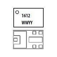
Package Dimensions 1612 WWYY 3.30±0.10 Top View Notes: 1. All dimensions are in millimeters. 2. Dimensions are inclusive of plating. 3. Dimensions are exclusive of mold flash and metal burr. PCB Land Patterns and Stencil Design 3.10 1.74 1.36 0.69 ...
Page 17
... USER FEED DIRECTION COVER TAPE Tape Dimensions (all dimension in mm MAX SECTION REF. 0. SECTION REF. R 0.65 Part Number Ordering Information Part # Qty ALM-1612-BLKG 100 ALM-1612-TR1G 3000 17 USER FEED DIRECTION 1612 1612 CARRIER WWYY WWYY TAPE TOP VIEW P10 ( REF. NOTES ...
Page 18
Reel Dimensions (13” reel DATE CODE EMBOSSED LETTERING 7.5mm HEIGHT EMBOSSED LINE (2x) 89.0mm LENGTH LINES 147.0mm AWAY FROM CENTER POINT ESD LOGO 6 PS RECYCLE LOGO SEE ...