RMPA5255 Fairchild Semiconductor, RMPA5255 Datasheet
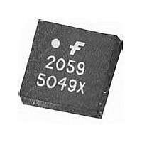
IC PWR AMP MOD 4.9-5.9GHZ 10-LCC

RMPA5255

Manufacturer Part Number
RMPA5255
Description
IC PWR AMP MOD 4.9-5.9GHZ 10-LCC
Manufacturer
Fairchild Semiconductor
Type
Power Amplifierr
Datasheet

Specifications of RMPA5255

Current - Supply
230mA
Frequency
4.9GHz ~ 5.9GHz
Gain
34dB
P1db
26dBm
Package / Case
11-LCC
Rf Type
WLL, WLAN
Voltage - Supply
3V ~ 3.6V
Number Of Channels
1
Frequency (max)
5.9GHz
Output Power
26dBm
Power Supply Requirement
Single
Single Supply Voltage (min)
3V
Single Supply Voltage (typ)
3.3V
Single Supply Voltage (max)
3.6V
Package Type
PLCC
Dual Supply Voltage (min)
Not RequiredV
Dual Supply Voltage (typ)
Not RequiredV
Dual Supply Voltage (max)
Not RequiredV
Supply Current
230mA
Pin Count
10
Mounting
Surface Mount
Lead Free Status / RoHS Status
Lead free / RoHS Compliant
Noise Figure
-
Test Frequency
-
Lead Free Status / Rohs Status
Compliant
Other names
RMPA5255TR

Available stocks

Company
Part Number
Manufacturer
Quantity
Price
Part Number:
RMPA5255
Manufacturer:
AD
Quantity:
1 433
Part Number:
RMPA5255
Manufacturer:
FAIRCHILD
Quantity:
51 860
Part Number:
RMPA5255
Manufacturer:
FAIRCHILD/仙童
Quantity:
20 000
©2005 Fairchild Semiconductor Corporation
RMPA5255 Rev. E
Electrical Characteristics
(176 µs burst time, 100 µs idle time) 54 Mbps Data Rate, 16.7 MHz Bandwidth
Notes:
1. VCC = 3.3V, VPC = 2.9V, T
2. Percentage includes system noise floor of EVM = 0.8%.
3. P
RMPA5255
4.9–5.9 GHz WLAN Linear Power Amplifier Module
Features
■ Full 4.9 to 5.9 GHz operation
■ 34 dB small signal gain
■ 230 mA total current at 18 dBm modulated power out
■ 2.3% EVM at 18 dBm modulated power out
■ 3.3 V collector supply voltage
■ Integrated power detector with 20 dB dynamic range
■ RoHS compliant 5 x 5 x 1.5 mm leadless package
■ Internally matched to 50 Ω and DC blocked RF
■ Internal DC bias de-coupling
■ Optimized for use in 802.11a applications
Frequency
Collector Supply Voltage
Mirror Supply Voltage
Mirror Supply Current
Gain
Total Current @ 18dBm Pout
EVM @ 18dBm Pout
Detector Output @ 18dBm Pout
Detector Threshold
input/output
OUT
measured at P
3
2
Parameter
IN
corresponding to power detection threshold.
A
= 25°C, PA is constantly biased, 50 Ω system.
Device
1 802.11a OFDM Modulation
1
Description
The RMPA5255 power amplifier module is designed for high
performance WLAN applications in the 4.9–5.9 GHz frequency
band. The 10 pin, 5 x 5 x 1.5 mm package with internal match-
ing on both input and output to 50 Ω , and internal bias network
components, allow for extremely simplified integration. An on-
chip detector provides power sensing capability. The PA’s low
power consumption and excellent linearity are achieved using
our InGaP Heterojunction Bipolar Transistor (HBT) technology.
Min
4.9
3.0
Typ
230
450
3.3
2.9
2.3
26
33
5
Max
5.9
3.6
September 2005
www.fairchildsemi.com
Units
GHz
dBm
mA
mA
mV
dB
%
V
V

Related parts for RMPA5255

RMPA5255 Summary of contents

Page 1

... Fairchild Semiconductor Corporation RMPA5255 Rev. E Description The RMPA5255 power amplifier module is designed for high performance WLAN applications in the 4.9–5.9 GHz frequency band. The 10 pin 1.5 mm package with internal match- ing on both input and output to 50 Ω , and internal bias network components, allow for extremely simplifi ...

Page 2

... Power Control bias current is included in the total quiescent current. 3. Measured from Device On signal turn on, (Logic Low) to the point where measured at P corresponding to power detection threshold. OUT IN Functional Block Diagram GND RF IN GND RMPA5255 Rev Single Tone Min 4.9 3.0 2.6 OUT PSense N ...

Page 3

... GHz 5.1 GHz 5.3 GHz 5.5 GHz 5.7 GHz 30 5.9 GHz Single Tone Power Out (dBm) RMPA5255 Rev RMPA5255 Detector Voltage vs. Modulated Pout 800 700 600 500 400 300 4.5 3 RMPA5255 Gain vs. Modulated Pout VCC=3.3V, VPC=2.9V, T=25°C 4.9 GHz 5 ...

Page 4

... Schematic 50Ω 3 Package Outline I/O 1 INDICATOR 1 2 TOP VIEW 3 FRONT VIEW 1.80 TYP. 0.70 TYP. 0.10 TYP. 1.70 TYP. 2 0.40 TYP. 1 BOTTOM VIEW RMPA5255 Rev. E VDET (P-Sense OUT 7 50Ω 220pF C2 0.01µF C3 2.2µF VPC VCC NOTES: 5.00 ±0.10mm 1. PACKAGE BASE MATERIAL AND ...

Page 5

... Pin Current VCC <1 nA Recommended turn-off sequence: Use reverse order described in the turn-on sequence above. Note: 1. Turn on sequence is not critical and it is not necessary to sequence power supplies in actual system level design. RMPA5255 Rev. E Actual Board Size = 2.0" X 1.5" www.fairchildsemi.com ...

Page 6

... RMPA5255 Rev. E Solder Materials & Temperature Profile: Reflow soldering is the preferred method of SMT attachment. Hand soldering is not recommended. Reflow Profile • Ramp-up: During this stage the solvents are evaporated from the solder paste. Care should be taken to prevent rapid oxidation (or paste slump) and solder bursts caused by violent solvent out-gassing. A maximum heating rate is 3° ...

Page 7

... PRODUCT STATUS DEFINITIONS Definition of Terms Datasheet Identification Advance Information Preliminary No Identification Needed Obsolete RMPA5255 Rev. E ISOPLANAR™ PowerSaver™ PowerTrench  LittleFET™ QFET  MICROCOUPLER™ QS™ MicroFET™ QT Optoelectronics™ ...

Related keywords