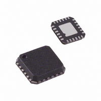
ADL5387ACPZ-R7 Analog Devices Inc, ADL5387ACPZ-R7 Datasheet - Page 16

ADL5387ACPZ-R7
Manufacturer Part Number
ADL5387ACPZ-R7
Description
IC QUADRATUR DEMOD 50MHZ 24LFCSP
Manufacturer
Analog Devices Inc
Datasheet
1.ADL5387ACPZ-R7.pdf
(28 pages)
Specifications of ADL5387ACPZ-R7
Function
Demodulator
Lo Frequency
100MHz ~ 2GHz
Rf Frequency
50MHz ~ 2GHz
P1db
12.8dBm
Gain
3.8dB
Noise Figure
16.5dB
Current - Supply
180mA
Voltage - Supply
4.75 V ~ 5.25 V
Package / Case
24-VFQFN, 24-CSP Exposed Pad
Frequency Range
50MHz To 2GHz
Rf Type
Quadrature
Supply Voltage Range
4.75V To 5.25V
Rf Ic Case Style
LFCSP
No. Of Pins
24
Operating Temperature Range
-40°C To +85°C
Frequency Max
2GHz
Lead Free Status / RoHS Status
Lead free / RoHS Compliant
Other names
ADL5387ACPZ-R7TR
Available stocks
Company
Part Number
Manufacturer
Quantity
Price
Company:
Part Number:
ADL5387ACPZ-R7
Manufacturer:
ADI
Quantity:
7 800
ADL5387
RF INPUT
The RF inputs have a differential input impedance of
approximately 50 Ω. For optimum performance, the RF port
should be driven differentially through a balun. The recommended
balun is M/A-COM ETC1-1-13. The RF inputs to the device
should be ac-coupled with 1000 pF capacitors. Ground-referenced
choke inductors must also be connected to RFIP and RFIN
(recommended value = 120 nH, Coilcraft 0402CS-R12XJL) for
appropriate biasing. Several important aspects must be taken
into account when selecting an appropriate choke inductor for
this application. First, the inductor must be able to handle the
approximately 40 mA of standing dc current being delivered
from each of the RF input pins (RFIP, RFIN). (The suggested
0402 inductor has a 50 mA current rating). The purpose of the
choke inductors is to provide a very low resistance dc path to
ground and high ac impedance at the RF frequency so as not to
affect the RF input impedance. A choke inductor that has a self-
resonant frequency greater than the RF input frequency ensures
that the choke is still looking inductive and therefore has a more
predictable ac impedance (jωL) at the RF frequency. Figure 48
shows the RF input configuration.
RF INPUT
ETC1-1-13
Figure 48. RF Input
120nH
120nH
1000pF
1000pF
21
22
RFIN
RFIP
Rev. 0 | Page 16 of 28
The differential RF port return loss has been characterized as
shown in Figure 49.
BASEBAND OUTPUTS
The baseband outputs QHI, QLO, IHI, and ILO are fixed
impedance ports. Each baseband pair has a 50 Ω differential
output impedance. The outputs can be presented with differential
loads as low as 200 Ω (with some degradation in linearity and
gain) or high impedance differential loads (500 Ω or greater
impedance yields the same excellent linearity) that is typical of
an ADC. The TCM9-1 9:1 balun converts the differential IF
output to single-ended. When loaded with 50 Ω, this balun
presents a 450 Ω load to the device. The typical maximum
linear voltage swing for these outputs is 2 V p-p differential.
The bias level on these pins is equal to VPOS − 2.8 V. The
output 3 dB bandwidth is 240 MHz. Figure 50 shows the
baseband output configuration.
–10
–12
–14
–16
–18
–20
–22
–24
–26
–28
0
0.2
Figure 50. Baseband Output Configuration
Figure 49. Differential RF Port Return Loss
QLO
0.4
QHI
ILO
IHI
16
15
14
13
0.6
FREQUENCY (GHz)
0.8
1.0
1.2
QHI
QLO
IHI
ILO
1.4
1.6
1.8
2.0


