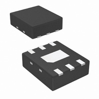
LMV225SD/NOPB National Semiconductor, LMV225SD/NOPB Datasheet - Page 24

LMV225SD/NOPB
Manufacturer Part Number
LMV225SD/NOPB
Description
IC DETECTOR RF POWER 6-LLP
Manufacturer
National Semiconductor
Datasheet
1.LMV225TLNOPB.pdf
(28 pages)
Specifications of LMV225SD/NOPB
Frequency
450MHz ~ 2GHz
Rf Type
Cellular, CDMA, W-CDMA
Input Range
-30dBm ~ 0dBm
Accuracy
1dB
Voltage - Supply
2.7 V ~ 5 V
Current - Supply
8mA
Package / Case
6-LLP
Pin Count
6
Screening Level
Industrial
Package Type
LLP EP
Lead Free Status / RoHS Status
Lead free / RoHS Compliant
Other names
LMV225SD/NOPB
LMV225SDTR
LMV225SDTR
Available stocks
Company
Part Number
Manufacturer
Quantity
Price
Part Number:
LMV225SD/NOPB
Manufacturer:
TI/德州仪器
Quantity:
20 000
www.national.com
Application Notes
The output voltage variation ∆V
input signals that fall within the linear range (in dB) of the
detector. In other words, the output variation is independent
of the absolute RF input signal:
In which V
error is usually much smaller than the ripple due to AM
modulation. In case of the LMV225/LMV228, V
dB. With ∆P
valid for all V
Output Ripple with Additional Filtering
The calculated result above is for an unfiltered configuration.
When a low pass filter is used by shunting a capacitor of e.g.
C
ground, this ripple is further attenuated. The cut-off fre-
quency follows from:
With the output resistance of the LMV225/LMV228 R
19.8 kΩ typical and C
equals f
ated by 5.36/100 or 25.4 dB. The remaining ripple will be
less than 20 mV. With a slope of 40 mV/dB this translates
into an error of less than
low output impedance buffer, a capacitor to reduce the ripple
will not be effective.
Output Ripple Measurement
Figure 6 shows the ripple reduction that can be achieved by
adding additional capacitance at the output of the LMV225/
LMV228. The RF signal of 900 MHz is AM modulated with a
100 kHz sinewave and a modulation index of 0.3. The RF
input power is swept while the modulation index remains
unchanged. Without the output capacitor the ripple is about
200 mV
ground, results in a ripple of 12 mV
OUT
= 1.5 nF at the output of the LMV225/LMV228 to
PP
C
FIGURE 5. V
= 5.36 kHz. A 100 kHz AM signal then gets attenu-
. Connecting a capacitor of 1.5 nF at the output to
Y
is the slope of the curve. The log-conformance
IN
OUT
= 5 dB for CDMA, ∆V
.
∆V
OUT
OUT
O
±
vs. RF Input Power P
= V
0.5 dB. Since the LMV226 has a
= 1.5 nF, the cut-off frequency
Y
OUT
· ∆P
(Continued)
OUT
PP
IN
is thus identical for RF
. The attenuation with
= 200 mV
Y
IN
PP
= 40 mV/
20076018
. This is
O
(7)
(8)
=
24
a 1.5 nF capacitor is then 20 • log (200/12) = 24.4 dB. This
is very close to the calculated number of the previous para-
graph.
PRINCIPLE OF OPERATION
The logarithmic response of the LMV225/LMV226/LMV228
is implemented by a logarithmic amplifier as shown in Figure
7. The logarithmic amplifier consists of a number of cas-
caded linear gain cells. With these gain cells, a piecewise
approximation of the logarithmic function is constructed.
Every gain cell has a response according to Figure 8. At a
certain threshold (E
means that the gain drops to zero. The output of gain cell 1
is connected to the input of gain cell 2 and so on.
FIGURE 6. Output Ripple vs. RF Input Power
FIGURE 7. Logarithmic Amplifier
K
), the gain cell starts to saturate, which
20076025
20076019


