RF2374PCBA-410 RFMD, RF2374PCBA-410 Datasheet - Page 3
RF2374PCBA-410
Manufacturer Part Number
RF2374PCBA-410
Description
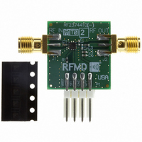
BOARD EVAL FOR RF2374
Manufacturer
RFMD
Type
Amplifierr
Datasheet
1.RF2374TR7.pdf
(13 pages)
Specifications of RF2374PCBA-410
Frequency
800MHz ~ 4GHz
For Use With/related Products
RF2374
Lead Free Status / RoHS Status
Lead free / RoHS Compliant
Other names
689-1037


DS101118
CDMA Low Noise Amplifier
HIGH GAIN MODE
Frequency
Gain
Noise Figure
Input IP3
Current Drain
Low Band LNA
HIGH GAIN MODE
Frequency
Gain
Gain
Noise Figure
Noise Figure
Input IP3
Power Supply
Voltage (V
Gain Select Low Level
(High Gain Mode)
Gain Select High Level
(Bypass Mode)
Gain Select On/Off Time
Power Down
Bias note: Due to the presence of ESD protection circuitry on the RF2374, the maximum allowable collector bias voltage (pin 6) is 4.0V. Higher
Bias note 2: In bypass mode, V
supply voltages such as 5V are permissible if a series resistor is used to drop V
to 2mA supplied by V
CC
Parameter
)
REF
.
REF
7628 Thorndike Road, Greensboro, NC 27409-9421 · For sales or technical
support, contact RFMD at (+1) 336-678-5570 or sales-support@rfmd.com.
is essentially a “don’t care” condition. Pulling V
Min.
869
1.6
50
0
Specification
Typ.
+2.0
+2.0
1.0
2.5
1.5
19
20
19
7
3
Max.
<150
894
950
0.8
5
REF
CC
Unit
nSec
dBm
dBm
MHz
MHz
mA
dB
dB
dB
dB
dB
dB
μA
low when in bypass mode does conserve the small 1mA
to <4.0V for a given I
V
V
V
IIP3 will improve if I
88MHz
870MHz
88MHz
870MHz
IIP3 will improve if I
High Gain mode.
Gain Select<0.8V, V
Low Gain mode.
Gain Select>1.6V, V
(C1 values range from 3 to 10pF),
Temp=-40°C to +85°C, and over process
Gain Select<0.8V, V
CC
.
Condition
CC
CC
REF
REF
REF
is raised above 7mA.
is raised above 7mA.
RF2374
: see bias note 2
=3V (typical)
=0V, V
CC
=3.0V
3 of 13
Related parts for RF2374PCBA-410
Image
Part Number
Description
Manufacturer
Datasheet
Request
R

Part Number:
Description:
3v Low Noise Amplifier Rf2374
Manufacturer:
RF Micro Devices
Datasheet:

Part Number:
Description:
IC AMP HBT GAAS CATV 8-SOIC
Manufacturer:
RFMD
Datasheet:

Part Number:
Description:
IC AMP MMIC GAAS 12GHZ 4-MICROX
Manufacturer:
RFMD
Datasheet:

Part Number:
Description:
IC AMP 3V LOW-NOISE SOT23-6
Manufacturer:
RFMD
Datasheet:

Part Number:
Description:
KIT EVAL FOR NBB-310
Manufacturer:
RFMD
Datasheet:
Part Number:
Description:
IC AMPLIFIER MMIC LNA 8-QFN
Manufacturer:
RFMD
Datasheet:
Part Number:
Description:
IC AMP MMIC GAAS 4GHZ 4-MICROX
Manufacturer:
RFMD
Datasheet:
Part Number:
Description:
IC SWITCH 10W PHEMT SPDT 12QFN
Manufacturer:
RFMD
Datasheet:
Part Number:
Description:
IC QUADRATURE MODULATOR 16-SOIC
Manufacturer:
RFMD
Datasheet:
Part Number:
Description:
100MHZ TO 4000MHZ, GAAS PHEMT MMIC LOW NOISE AMPLIFIERS
Manufacturer:
RFMD
Part Number:
Description:
KIT EVAL FOR RF2336
Manufacturer:
RFMD
Datasheet:


Part Number:
Description:
IC AMP WLAN/LNA DVR 3V SOT23-5
Manufacturer:
RFMD
Datasheet:

Part Number:
Description:
IC AMP HBT GAAS LNA BYPASS 8-QFN
Manufacturer:
RFMD
Datasheet: