AA003053-G Navman Wireless, AA003053-G Datasheet - Page 5
AA003053-G
Manufacturer Part Number
AA003053-G
Description
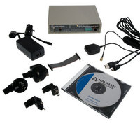
DEV KIT FOR JUPITER 30XLP
Manufacturer
Navman Wireless
Type
Receiver, GPSr
Specifications of AA003053-G
Frequency
1575.42MHz
For Use With/related Products
Jupiter 30XLP
Lead Free Status / RoHS Status
Lead free / RoHS Compliant
Other names
943-1000


2.2 Receiver architecture
The functional architecture of the Jupiter 30 xLP receiver is shown in Figure 2-1.
V_ANT
2.3 Major components of the Jupiter 30 xLP
LNA (Low Noise Amplifier):
receiver to use a passive antenna. A very low noise design is used to provide maximum
sensitivity.
LNA switch:
Bias T:
Bandpass SAW filter (1.575 GHz):
by external influences that would corrupt the operation of the receiver. The filtered signal is fed
to the RF input of GSC3 chipset for further processing. The filter has a bandwidth of 2 MHz.
TCXO (Temperature Compensated Crystal Oscillator):
controls the down conversion process for the RFIC block.
Regulator:
and the digital IO section of the GSC3 chip.
Main power:
Brown out detector:
the module in case of any drop in the voltage. This detector chip also serves the function of
power-on-reset.
OR-ing circuit:
or the back-up voltage input in order for the RTC/SRAM elements to work in low power and
continuous modes. However a back-up voltage must be connected if the device is to be shut
down and expected to perform Hot and Warm starts.
VDD_RTC regulator:
Battery power:
circuit, and provides the power to the battery-backed SRAM and the RTC section of the GSC3.
LA000576D © 2008 Navman Wireless OEM Solutions. All rights reserved. Proprietary information and specifications subject to change without notice.
bias T
input
active or passive antenna
this provides the voltage to an external active antenna.
this dual low-noise regulator provides two outputs of 2.85 V power to the RF section
this switch controls the LNA during low power modes.
primary supply voltage range is 3.0–3.6 V.
LNA
switch
LNA
this circuit distributes the RTC/SRAM voltage from either the main voltage supply
the back-up battery supply feeds the VDD_RTC regulator through the OR-ing
the precision voltage detector chip senses the input voltage and resets
supplies a regulated voltage for the RTC/SRAM cell within the GSC3 chip.
TCXO
SAW
filter
this amplifies the GPS signal and provides enough gain for the
Figure 2-1: Jupiter 30 xLP architecture
this filters the GPS signal removing unwanted signals caused
RTC crystal
XTAL_IN
RFIN
LNA_EN
VCC_RF
controls/
GPIO
regulator
this highly stable 16.369 MHz oscillator
UART
ports
combined RF/baseband device
VDD_BB
GSC3e LPx
3.0 - 3.6 V in
brown-out
SRESET
detector
power
main
AD [0-18]
4 Mb Flash
VDD_RTC
D [0-15]
VDD_RTC
regulator
OR-ing
circuit
CTRL
1.9 - 3.6 V
battery
power
Related parts for AA003053-G
Image
Part Number
Description
Manufacturer
Datasheet
Request
R

Part Number:
Description:
ANTENNA GPS ACTIVE 5M CABLE
Manufacturer:
Navman Wireless
Datasheet:

Part Number:
Description:
DEV KIT FOR JUPITER 32XLP
Manufacturer:
Navman Wireless
Datasheet:

Part Number:
Description:
DEV KIT FOR JUPITER 3 AND J3-30
Manufacturer:
Navman Wireless
Datasheet:

Part Number:
Description:
TERMINAL MDT-860 MOBILE DATA
Manufacturer:
Navman Wireless
Datasheet:


Part Number:
Description:
MODULE GPS RECEIVER JUPITER 3
Manufacturer:
Navman Wireless
Datasheet:

Part Number:
Description:
MODULE GPS JUPITER 30XLP 20CH
Manufacturer:
Navman Wireless
Datasheet:

Part Number:
Description:
MODULE GPS JUPITER 32XLP 20CH
Manufacturer:
Navman Wireless
Datasheet:

Part Number:
Description:
MODULE GPS RECEIVER JUPITER 3-30
Manufacturer:
Navman Wireless
Datasheet:

Part Number:
Description:
MODULE JUPITER 31 GPS W/R/A OSX
Manufacturer:
Navman Wireless
Datasheet:

Part Number:
Description:
MODULE GPS RECEIVER JUPITER 2
Manufacturer:
Navman Wireless
Datasheet:

Part Number:
Description:
DEV KIT FOR MDT860
Manufacturer:
Navman Wireless
Datasheet:

Part Number:
Description:
EVAL KIT GPS JUPITER 2
Manufacturer:
Navman Wireless
Datasheet: