J3,30DK,00,3.5 Navman Wireless, J3,30DK,00,3.5 Datasheet - Page 4
J3,30DK,00,3.5
Manufacturer Part Number
J3,30DK,00,3.5
Description
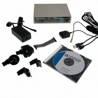
DEV KIT FOR JUPITER 3 AND J3-30
Manufacturer
Navman Wireless
Type
Receiver, GPSr
Datasheet
1.J330DK003.5.pdf
(17 pages)
Specifications of J3,30DK,00,3.5
Frequency
1575.42MHz
For Use With/related Products
Jupiter 3, J3-30
Lead Free Status / RoHS Status
Lead free / RoHS Compliant
Other names
943-1006


Jupiter 3-30
2.2 Receiver architecture
The functional architecture of the Jupiter 3-30 receiver is shown in Figure 2-1.
2.3 Major components of the Jupiter 3-30
lna(lownoiseamplifier): this amplifies the GPS signal and provides enough gain for the receiver to use a passive antenna.
A very low noise design is used to provide maximum sensitivity.
lnaswitch: this switch controls the LNA during low power modes.
Biast: this provides the voltage to an external active antenna.
BandpassSaWfilter(1.575GHz): this filters the GPS signal removing unwanted signals caused by external influences that
would corrupt the operation of the receiver. The filtered signal is fed to the RF input of GSC3 chipset for further processing.
The filter has a bandwidth of 2 MHz.
tCXo(temperatureCompensatedCrystaloscillator): this highly stable 16.369 MHz oscillator controls the down conversion
process for the RFIC block.
regulator: this dual low-noise regulator provides two outputs of 2.85 V power to the RF section and the digital IO section of
the GSC3 chip.
mainpower: primary supply voltage range is 3.0–3.6 V.
Brownoutdetector: the precision voltage detector chip senses the input voltage and resets the module in case of any drop in
the voltage. This detector chip also serves the function of power-on-reset.
or-ingcircuit: this circuit distributes the RTC/SRAM voltage from either the main voltage supply or the back-up voltage
input in order for the RTC/SRAM elements to work in low power and continuous modes. However a back-up voltage must be
connected if the device is to be shut down and expected to perform Hot and Warm starts.
Vdd_rtCregulator: supplies a regulated voltage for the RTC/SRAM cell within the GSC3 chip.
Batterypower: the back-up battery supply feeds the VDD_RTC regulator through the OR-ing circuit, and provides the power
to the battery-backed SRAM and the RTC section of the GSC3.
V_ANT
bias T
input
V
active or passive antenna
switch
LNA
LNA
Navman Wireless OEM Solutions • 27171 Burbank -Suite 200; Foothill Ranch, CA 92610-2501
TEL: +(949) 461-7150 • FAX: +(949) 461-7860 • www.navmanwirelessoem.com
|
Datasheet
SAW Filter
TCXO
Figure 2-1: Jupiter 3-30 architecture
RTC crystal
LNA_EN
XTAL_IN
RFIN
VCC_RF
regulator
Controls
GPIO/
combined RF/baseband device
VDD_BB
GSC3f/LPx
UART
ports
3.0 – 3.6V in
brown-out
detector
power
SRESET
main
VDD_RTC
VDD_RTC
regulator
OR-ing
Circuit
1.9 – 3.6V
battery
power
2
Related parts for J3,30DK,00,3.5
Image
Part Number
Description
Manufacturer
Datasheet
Request
R

Part Number:
Description:
ANTENNA GPS ACTIVE 5M CABLE
Manufacturer:
Navman Wireless
Datasheet:

Part Number:
Description:
DEV KIT FOR JUPITER 32XLP
Manufacturer:
Navman Wireless
Datasheet:

Part Number:
Description:
DEV KIT FOR JUPITER 30XLP
Manufacturer:
Navman Wireless
Datasheet:

Part Number:
Description:
TERMINAL MDT-860 MOBILE DATA
Manufacturer:
Navman Wireless
Datasheet:


Part Number:
Description:
MODULE GPS RECEIVER JUPITER 3
Manufacturer:
Navman Wireless
Datasheet:

Part Number:
Description:
MODULE GPS JUPITER 30XLP 20CH
Manufacturer:
Navman Wireless
Datasheet:

Part Number:
Description:
MODULE GPS JUPITER 32XLP 20CH
Manufacturer:
Navman Wireless
Datasheet:

Part Number:
Description:
MODULE GPS RECEIVER JUPITER 3-30
Manufacturer:
Navman Wireless
Datasheet:

Part Number:
Description:
MODULE JUPITER 31 GPS W/R/A OSX
Manufacturer:
Navman Wireless
Datasheet:

Part Number:
Description:
MODULE GPS RECEIVER JUPITER 2
Manufacturer:
Navman Wireless
Datasheet:

Part Number:
Description:
DEV KIT FOR MDT860
Manufacturer:
Navman Wireless
Datasheet:

Part Number:
Description:
EVAL KIT GPS JUPITER 2
Manufacturer:
Navman Wireless
Datasheet: