MCP2030DM-TPR Microchip Technology, MCP2030DM-TPR Datasheet - Page 25
MCP2030DM-TPR
Manufacturer Part Number
MCP2030DM-TPR
Description
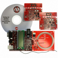
BOARD DEMO PICTAIL MCP2030
Manufacturer
Microchip Technology
Type
Front Endr
Specifications of MCP2030DM-TPR
Frequency
125kHz
For Use With/related Products
MCP2030
Lead Free Status / RoHS Status
Not applicable / Not applicable
Lead Free Status / RoHS Status
Lead free / RoHS Compliant, Not applicable / Not applicable


3.0
TABLE 3-1:
3.1
The V
digital circuitry within the MCP2030. This pin requires
an appropriate bypass capacitor of 0.1 µF. The voltage
on this pin should be maintained in the 2.0V-3.6V range
for specified operation.
The V
path for both analog and digital circuitry of the
MCP2030. If an analog ground plane is available, it is
recommended that this device be tied to the analog
ground plane of the PCB.
3.2
The CS pin needs to stay high when the device is
receiving input signals. Leaving the CS pin low will
place the device in the SPI Programming mode.
The CS pin is an open collector output. This pin has an
internal pull-up resistor to ensure that no spurious SPI
communication occurs between power-up and pin
configuration of the MCU.
© 2005 Microchip Technology Inc.
Type Identification: I = Input; O = Output; P = Power
Pin No.
10
11
12
13
14
DD
1
2
3
4
5
6
7
8
9
SS
PIN DESCRIPTIONS
Supply Voltage (V
Chip Select (CS)
pin is the power supply pin for the analog and
pin is the ground pin and the current return
LFDATA/CCLK/SDIO
PIN FUNCTION TABLES
SCLK/ALERT
Symbol
LCCOM
RSSI
LCY
LCX
V
V
LCZ
V
V
CS
NC
NC
DD
DD
SS
SS
DD
, V
SS
)
I/O/P
N/A
N/A
I/O
I/O
O
P
P
P
P
I
I
I
I
I
Ground Pin.
Chip Select Digital Input Pin.
Clock input for the modified 3-wire SPI interface.
ALERT output: This pin goes low if there is a parity error in the
Configuration register or the 32 ms alarm timer is timed out.
Received Signal Strength Indicator (RSSI) current output.
No Connect.
Demodulated data output.
Carrier clock output.
Serial input or output data for the modified 3-wire SPI interface.
Positive Supply Voltage Pin.
Positive Supply Voltage Pin.
Input pin for external LC antennas.
Input pin for external LC antennas.
Input pin for external LC antennas.
No Connect.
Common reference input for the external LC antennas.
Ground Pin.
3.3
This pin becomes the SPI clock input (SCLK) when CS
is low, and becomes the ALERT output when CS is
high.
The ALERT pin is an open collector output. This pin has
an internal pull-up resistor to ensure that no spurious
SPI communication occurs between power-up and pin
configuration of the MCU.
3.4
This pin becomes the Received Signal Strength Indicator
(RSSI) output current sink when the RSSI output option
is selected.
SPI Clock Input (SCLK/ALERT)
Received Signal Strength
Indicator (RSSI)
Function
MCP2030
DS21981A-page 25
Related parts for MCP2030DM-TPR
Image
Part Number
Description
Manufacturer
Datasheet
Request
R

Part Number:
Description:
IC KEYLESS ENTRY AFE 14TSSOP
Manufacturer:
Microchip Technology
Datasheet:

Part Number:
Description:
IC KEYLESS ENTRY AFE 14SOIC
Manufacturer:
Microchip Technology
Datasheet:

Part Number:
Description:
IC KEYLESS ENTRY AFE 14DIP
Manufacturer:
Microchip Technology
Datasheet:
Part Number:
Description:
3D ANALOG TRANSPONDER (AFE), -40C to +125C, 14-PDIP, TUBE
Manufacturer:
Microchip Technology
Datasheet:

Part Number:
Description:
Three-channel Analog Front-end Device
Manufacturer:
Microchip Technology Inc.
Datasheet:
Part Number:
Description:
Manufacturer:
Microchip Technology Inc.
Datasheet:
Part Number:
Description:
Manufacturer:
Microchip Technology Inc.
Datasheet:
Part Number:
Description:
Manufacturer:
Microchip Technology Inc.
Datasheet:
Part Number:
Description:
Manufacturer:
Microchip Technology Inc.
Datasheet:
Part Number:
Description:
Manufacturer:
Microchip Technology Inc.
Datasheet:
Part Number:
Description:
Manufacturer:
Microchip Technology Inc.
Datasheet: