RF2713PCK-M RFMD, RF2713PCK-M Datasheet - Page 7
RF2713PCK-M
Manufacturer Part Number
RF2713PCK-M
Description
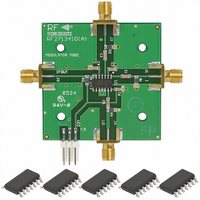
KIT EVAL FOR RF2713 MODULATOR
Manufacturer
RFMD
Type
Modulator, Demodulatorr
Datasheet
1.RF2713PCK-D.pdf
(16 pages)
Specifications of RF2713PCK-M
Frequency
0Hz ~ 250MHz
For Use With/related Products
RF2713 MODULATOR
Lead Free Status / RoHS Status
Lead free / RoHS Compliant
Other names
689-1042
Available stocks
Company
Part Number
Manufacturer
Quantity
Price
Company:

Part Number:
RF2713PCK-M
Manufacturer:
RFMD
Quantity:
5 000


Rev A6 DS080403
Pin
10
11
12
13
14
7
8
9
LO INPUT
Function
Q IF OUT
Q OUT
I OUT
GND
GND
GND
VCC
Description (Modulator Configuration)
Same as pin 6, except complementary input.
Pins 8 and 9 are not used in a normal quadrature modulator application,
and are left unconnected. Note, however, that the outputs of each of these
pins are independent upconverted I and Q channels. These signals may be
useful in other applications where independent IF channels are needed.
Also note that these outputs are optimized as baseband outputs for the
demodulator configuration. As a result, the gain rolls-off quickly with
increasing frequency. This gain roll-off will limit the usefulness of these
pins as independent I and Q upconverters. If these outputs are to be used,
please refer to the Demodulator pin descriptions regarding load imped-
ances.
Same as pin 8, except Q Mixer’s Output.
Ground connection. Keep traces physically short and connect immediately
to ground plane for best performance.
Same as pin 10.
Same as pin 10.
High impedance, single-ended modulator LO input. The LO applied to this
pin is frequency divided by a factor of 2 and becomes the "Carrier". For
modulation, the Carrier is the center of the modulated output spectrum
(except in the case of SSB/SC). The input impedance is determined by an
internal 500Ω bias resistor to V
be provided if the pin is connected to a device with DC present. Matching
the input impedance is typically achieved by adding a 51Ω resistor to
ground on the source side of the AC coupling capacitor. For the LO input,
maximum power transfer is not critical. The internal LO switching circuits
are controlled by the voltage, not power, into the part. In cases where the
LO source does not have enough available voltage, a reactive match (volt-
age transformer) can be used. The LO circuitry consists of a limiting ampli-
fier followed by a digital divider. The limiting amp ensures that the flip-flop
type divider is driven with a square wave over a wide range of input levels.
Because the flip-flop uses the rising and falling edges of the limiter output,
the quadrature accuracy of the Carrier supplied to the mixers is directly
related to the duty cycle, or equivalently to the even harmonic content, of
the input LO signal. In particular, care should be taken to ensure that the
2xLO level input to this pin is at least 20dB below the LO level. Otherwise,
the LO input is not sensitive to the type of input wave form, except for IF fre-
quencies below ~2.5MHz, in which case the LO input should be a square
wave, in order to ensure proper triggering of the flip-flops. IF frequencies
below 100kHz are attainable if the LO is a square wave and sufficiently
large DC blocking capacitors are used.
Voltage supply for the entire device. This pin should be well bypassed at all
frequencies (IF, LO, Carrier, Baseband) that are present in the part.
7628 Thorndike Road, Greensboro, NC 27409-9421 · For sales or technical
support, contact RFMD at (+1) 336-678-5570 or sales-support@rfmd.com.
CC
. An external blocking capacitor should
Interface Schematic
Same as pin 6.
Same as pin 8.
LO IN
RF2713
V
V
CC
CC
500 Ω
2 kΩ
I/Q OUT
V
CC
500 Ω
7 of 16
Related parts for RF2713PCK-M
Image
Part Number
Description
Manufacturer
Datasheet
Request
R

Part Number:
Description:
IC AMP HBT GAAS CATV 8-SOIC
Manufacturer:
RFMD
Datasheet:

Part Number:
Description:
IC AMP MMIC GAAS 12GHZ 4-MICROX
Manufacturer:
RFMD
Datasheet:

Part Number:
Description:
IC AMP 3V LOW-NOISE SOT23-6
Manufacturer:
RFMD
Datasheet:

Part Number:
Description:
KIT EVAL FOR NBB-310
Manufacturer:
RFMD
Datasheet:
Part Number:
Description:
IC AMPLIFIER MMIC LNA 8-QFN
Manufacturer:
RFMD
Datasheet:
Part Number:
Description:
IC AMP MMIC GAAS 4GHZ 4-MICROX
Manufacturer:
RFMD
Datasheet:
Part Number:
Description:
IC SWITCH 10W PHEMT SPDT 12QFN
Manufacturer:
RFMD
Datasheet:
Part Number:
Description:
IC QUADRATURE MODULATOR 16-SOIC
Manufacturer:
RFMD
Datasheet:
Part Number:
Description:
100MHZ TO 4000MHZ, GAAS PHEMT MMIC LOW NOISE AMPLIFIERS
Manufacturer:
RFMD
Part Number:
Description:
KIT EVAL FOR RF2336
Manufacturer:
RFMD
Datasheet:


Part Number:
Description:
IC AMP WLAN/LNA DVR 3V SOT23-5
Manufacturer:
RFMD
Datasheet:

Part Number:
Description:
IC AMP HBT GAAS LNA BYPASS 8-QFN
Manufacturer:
RFMD
Datasheet:

Part Number:
Description:
IC AMP MMIC GAAS 10GHZ 4-MICROX
Manufacturer:
RFMD
Datasheet: