AD8339-EVALZ Analog Devices Inc, AD8339-EVALZ Datasheet
AD8339-EVALZ
Specifications of AD8339-EVALZ


Related parts for AD8339-EVALZ


AD8339-EVALZ Summary of contents
Page 1
... During power-down, the serial interface remains active so that the device can be programmed again. The dynamic range is typically 160 dB/Hz at the I and Q outputs. The AD8339 is available × 6 mm, 40-lead LFCSP and is specified over the industrial temperature range of −40°C to +85°C. ...
Page 2
... Applications Information .............................................................. 24 Logic Inputs and Interfaces ....................................................... 24 Reset Input .................................................................................. 24 LO Input ...................................................................................... 24 Evaluation Board ............................................................................ 25 Connections to the Board ......................................................... 26 Test Configurations .................................................................... 26 AD8339-EVALZ Artwork ......................................................... 33 Outline Dimensions ....................................................................... 35 Ordering Guide .......................................................................... 35 Rev Page ...
Page 3
... A < +85°C ±0.1 A AD8339 Unit MHz MHz MHz dBm V °C kΩ||pF kΩ||pF mS dB/ dBm dBV dBc dBc dBm dBm dBm dB nV/√ ...
Page 4
... AD8339 Parameter LOGIC INTERFACES Pin SDI, Pin CSB, Pin SCLK, Pin RSET Logic Level High Logic Level Low Pin RSTS Logic Level High Logic Level Low Bias Current Input Resistance LO Divider RSET Setup Time LO Divider RSET High Pulse Width LO Divider RSET Response Time ...
Page 5
... V to GND device reliability. +0 − −1 GND ESD CAUTION VPOS − 1 32.2°C/W 17.8°C/W 2.7°C/W 0.3°C/W 16.7°C/W 150° −40°C to +85°C −65°C to +150°C 300°C Rev Page AD8339 ...
Page 6
... Exposed Pad. The exposed pad is not connected internally. For increased reliability of the solder joints and maximum thermal capability recommended that the pad be soldered to the ground plane RF2N 1 30 RF2P 2 29 PIN 1 COMM 3 INDICATOR 28 COMM 4 27 AD8339 SCLK 5 26 TOP VIEW CSB 6 25 (Not to Scale) VPOS 7 24 VPOS 8 23 RF3P RF3N ...
Page 7
... VPOS LOGIC RSTS INTERFACE COMM Figure 4. RSTS Logic Input VPOS 4LOP 4LON COMM Figure 5. Local Oscillator Inputs VPOS LODC COMM Figure 6. LO Decoupling Pin VPOS RFxP RFxN COMM Figure 7. RF Inputs Figure 8. Output Drivers Rev Page AD8339 COMM IxOP QxOP VNEG ...
Page 8
... AD8339 TYPICAL PERFORMANCE CHARACTERISTICS V = ± 25° MHz typical of all channels, differential voltages, dBm (50 Ω), phase select code = 0000, unless otherwise noted (see Figure 42). 1 1MHz CODE 0100 1.0 Q 0.5 CODE 1000 0 I –0.5 –1.0 CODE 1100 –1.5 –2.0 –1.5 –1.0 –0.5 ...
Page 9
... BASEBAND FREQUENCY (Hz) Frequency for All Channels and Codes (See Figure 44 10kHz –1 –2 –3 1M 10M RF FREQUENCY (Hz) First Quadrant, over the Range of Operating Temperatures 10kHz –2 –4 –6 –8 1M 10M RF FREQUENCY (Hz) First Quadrant, over the Range of Operating Temperatures AD8339 100k 50M 50M ...
Page 10
... AD8339 1.4 I OUTPUT OF CHANNEL 1 SHOWN TRANSCONDUCTANCE = [(V /787Ω)/V BB 1.3 1.2 1.1 1.0 PHASE DELAY = 0° 0.9 PHASE DELAY = 22.5° PHASE DELAY = 45° PHASE DELAY = 67.5° 0.8 1M 10M RF FREQUENCY (Hz) Figure 21. Transconductance vs. RF Frequency for First Quadrant Phase Delays 10 0 –10 – ...
Page 11
... Figure 32. Output Compliance Range for Four Values of Phase Delay Rev Page AD8339 10M 50M RF FREQUENCY (Hz 10M 50M RF FREQUENCY (Hz) GAIN = DELAY = 0° DELAY = 22.5° ...
Page 12
... AD8339 CH2 500mV CH3 1.00V Ω M200ns T 608.000ns Figure 33. Enable Response vs. CSB (Filter Disabled to Show Response) with a Previously Enabled Channel (See Figure 44 CH2 AMPL 1.82V CH3 1.00V Ω CH2 500mV M2.00µs T 7.840µs Figure 34. Enable Response vs. CSB (Filter Disabled to Show Response) with ...
Page 13
... Figure 39. Phase Switching Response at 180° (Top: CSB) 0 –10 –20 –30 –40 –50 VNEG –60 VPOS –70 –80 –90 –100 10k 100k 1M FREQUENCY (Hz) Figure 40. PSRR vs. Frequency (see Figure 51 640mV –50 10M 50M Rev Page AD8339 VPOS VNEG –30 – TEMPERATURE (°C) Figure 41. Supply Current vs. Temperature 90 ...
Page 14
... SIGNAL GENERATOR Figure 43. P1dB Test Circuit AD8334 LNA 20Ω FB 0.1µF RFxP IxOP AD8339 RFxN QxOP 0.1µF 20Ω 4LOP 50Ω SIGNAL GENERATOR Figure 44. Phase and Amplitude vs. Baseband Frequency Rev Page AD8021 787Ω 2.2nF OSCILLOSCOPE 2.2nF 787Ω ...
Page 15
... SIGNAL GENERATOR Figure 47. Noise Rev Page AD8021 787Ω IxOP OSCILLOSCOPE 787Ω QxOP 50Ω AD8021 SIGNAL GENERATOR OSCILLOSCOPE IxOP AD8339 50Ω 50Ω QxOP 4LOP 50Ω AD829 6.98kΩ 270pF SPECTRUM IxOP ANALYZER 270pF QxOP 6.98kΩ 50Ω AD829 AD8339 ...
Page 16
... SIGNAL GENERATOR Figure 49. OIP3 and IM3 vs. RF Frequency AD8334 LNA 20Ω FB 0.1µF RFxP IxOP AD8339 RFxN QxOP 0.1µF 20Ω 4LOP 50Ω SIGNAL GENERATOR Figure 50. Output Compliance Range Rev Page AD8021 787Ω 100pF SPECTRUM ...
Page 17
... SIGNAL VPOS GENERATOR VPOS RFxP IxOP AD8339 0.1µF RFxN QxOP 4LOP SIGNAL VPOS GENERATOR Figure 51. PSRR Rev Page SPECTRUM ANALYZER AD8339 ...
Page 18
... RSET synchronizes the LO dividers when multiple AD8339s are used in arrays; RSTS sets all the SPI port control bits to 0. RSTS is used for testing or to disable the AD8339 without the need to program it via the SPI port. The I and Q outputs are current-formatted and summed together for beamforming applications ...
Page 19
... Column 1 of Table 4 is defined as being between the baseband channel outputs example, for a common signal applied to a pair of RF inputs to an AD8339, the baseband outputs are in phase for matching phase codes. However, if the phase code for Channel 1 is 0000 and that of Channel 2 is 0001, then Channel 2 leads Channel 1 by 22.5° ...
Page 20
... The noise contributed by the AD8339 is then 11 nV/√Hz × 1.7 or ~18.7 nV/√Hz at the AD8021 output. The combined noise of the AD8021 and the 1.58 kΩ feedback resistor is 6.3 nV/√Hz, so the total output referred noise is approximately 19.7 nV/√ ...
Page 21
... AD8334 for the lowest power per channel. For optimum signal- to-noise performance, the output of the LNA is applied directly to the input of the AD8339. To sum the signals E1 through E4 shifted 45° relative setting the phase code in Channel 2 to 0010 shifted 90° (0100), and E4 is shifted 135° ...
Page 22
... SIGNAL +5V 0.1µF HPF 1100Hz – 1µF 698Ω ∑ AD8021 5.6nF 0.1µF –5V Figure 55. 16-Channel Beamformer Using the AD8339 Rev Page FROM OTHER AD8021 SECOND ORDER SUMMING AMPLIFIER R4 LPF2 +10V 81kHz 0.1µ – 698Ω ∑ AD797 –10V ...
Page 23
... When all four ENBL bits are low, only the SPI port is powered up. This feature allows for low power consumption (~13 mW per AD8339 or 3.25 mW per channel) when the CW Doppler function is not needed. Because the SPI port stays alive even with the rest of the chip powered down, the part can be awakened again by simply programming the port ...
Page 24
... The function of the RSET pin is to phase align all the LO signals in multiple AD8339s. The 4LO divider of each AD8339 can be initiated in one of four possible states: 0°, 90°, 180°, or 270° relative to other AD8339s. The internally generated I/Q signals of each AD8339 LO are always at a 90° ...
Page 25
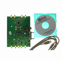
... AD8339. The RF input signals can be derived from three sources, user selectable by jumpers. Test points enable signal tracing at various circuit nodes. The AD8339-EVALZ requires bipolar 5 V power supplies. A 3.3 V on-board regulator provides power for the USB and EEPROM devices. The AD8339 is configured using the ...
Page 26
... AD9271 data sheet for setup details. The AD9271 evaluation board is attached to the AD8339 by inserting the three plastic standoffs into the three guide holes in the AD8339-EVALZ board; all the jumpers in P3 and P4 are AD9271 drive. removed. The bottom connectors of the AD9271 board engage P3 and P4 and route the LNA outputs of the AD9271 to the AD8339 ...
Page 27
... AD8334 LNA COMMON SIGNAL PATH Figure 59. AD8339 Test Configuration—Common Input Signal Drive Figure 60. AD8339-EVALZ with AD9271 Evaluation Board Attached as Input Source AD8339 Rev Page AD8339 ...
Page 28
... AD8339 TOP: SIGNAL GENERATOR FOR 4LO INPUT (FOR EXAMPLE, 20MHz, 1Vp-p) BOTTOM: SIGNAL GENERATOR FOR RF INPUT (FOR EXAMPLE, 5.01MHz) SYNCHRONIZE GENERATORS PERSONAL COMPUTER USB CABLE +5V Figure 61. AD8339-EVALZ Typical Test Setup Rev Page POWER SUPPLY –5V 4LO INPUT OUTPUTS ...
Page 29
... Table 7). As shipped, the evaluation board is configured to connect all the AD8339 RF inputs to a single LNA output. In this configur- ation, the phases of the four channels can be shifted throughout the full range and the outputs can be viewed on a multichannel scope using one of the channels as a reference ...
Page 30
... AD8339 L10 C67 IN1 120nH 0.1µF IN1S L7 IN2 120nH C60 0.1µF IN2S C8 22pF COM2 1 INH2 CFB2 18nF 2 LMD2 IDENTIFIER C43 RFB2 0.1µF 274Ω 3 COM2X R44 20Ω 4 LON2 LON2 R43 RF2 20Ω 5 LOP2 LOP2 C44 0.1µF 6 VIP2 C45 0.1µ ...
Page 31
... C51 R36 I4OP 0.1µF 0.1µF 5.23kΩ VNEG R30 R2 4.22kΩ 0Ω COMPONENTS SHOWN IN GRAY ARE NOT INSTALLED ENGAGES WITH CONNECTOR ON AD9271 EVAL BOARD P3 Rev Page AD8339 R16 787Ω C25 0.1µF C83 2. 2nF R17 0Ω 6 AD8021 C84 ...
Page 32
... AD8339 L11 1µF 120nH 10V + C78 C77 0.1µF 0.1µ OUT GND A6 OUT TAB ADP3339AKCZ-3 RDY0/SLRD 2 NC RDY1/SLWR 3. AVCC C69 24MHz 0.1µF 4 XTALOUT 5 XTALIN 12pF AGND A7 7 3.3V AVCC USB C70 8 TYPE B D+ 0.1µF DPLUS D– DMINUS GND ...
Page 33
... AD8339-EVALZ ARTWORK Figure 66 through Figure 69 show the artwork for the AD8339-EVALZ. Figure 66. AD8339-EVALZ Component Side Copper Figure 67. AD8339-EVALZ Wiring Side Copper Rev Page AD8339 ...
Page 34
... AD8339 Figure 68. AD8339-EVALZ Component Side Silkscreen Figure 69. AD8339-EVALZ Assembly Rev Page ...
Page 35
... PLANE ORDERING GUIDE Model Temperature Range 1 AD8339ACPZ −40°C to +85°C 1 AD8339ACPZ-R7 −40°C to +85°C 1 AD8339ACPZ-RL −40°C to +85°C 1 AD8339-EVALZ RoHS Compliant Part. 0.60 MAX 0.50 BSC 5.75 BSC SQ 0.50 0.40 0.30 0.80 MAX 0.65 TYP 0.05 MAX 0.02 NOM ...
Page 36
... AD8339 NOTES ©2007–2009 Analog Devices, Inc. All rights reserved. Trademarks and registered trademarks are the property of their respective owners. D06587-0-2/09(A) Rev Page ...