SDBC-DK3 Silicon Laboratories Inc, SDBC-DK3 Datasheet
SDBC-DK3
Specifications of SDBC-DK3


Related parts for SDBC-DK3

SDBC-DK3 Summary of contents
Page 1
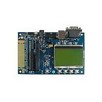
... USB type B connector with Silicon Labs CP2102 USB > Serial Converter onboard On board 3.3 V PSU through hole breadboard area for customer's application Rev. 0.4 8/ Figure 2. MSC-DBLB2 (Not Included) Testing Platform for controlled Lab Tests Copyright © 2009 by Silicon Laboratories K U ’ UID E (Loadboard) SDBC-DK3 UG ...
Page 2
... SDBC-DK3 UG 2 Rev. 0.4 ...
Page 3
... Results (PER Test .38 7.3. Additional Information . . . . . . . . . . . . . . . . . . . . . . . . . . . . . . . . . . . . . . . . . . . . . . . . 39 7.3.1. USB Communications . . . . . . . . . . . . . . . . . . . . . . . . . . . . . . . . . . . . . . . . . . . . 39 7.3.2. Packet Structure . . . . . . . . . . . . . . . . . . . . . . . . . . . . . . . . . . . . . . . . . . . . . . . . 40 8. Custom Software Development . . . . . . . . . . . . . . . . . . . . . . . . . . . . . . . . . . . . . . . . . . . . 41 8.1. Program Structure . . . . . . . . . . . . . . . . . . . . . . . . . . . . . . . . . . . . . . . . . . . . . . . . . . . 41 8.1.1. Basic Code Overview . . . . . . . . . . . . . . . . . . . . . . . . . . . . . . . . . . . . . . . . . . . .45 8.2. Basic Hardware Connections . . . . . . . . . . . . . . . . . . . . . . . . . . . . . . . . . . . . . . . . . . 46 9. Main . . . . . . . . . . . . . . . . . . . . . . . . . . . . . . . . . . . . . . . . . . . . . . . . . . . . . . . . . . . . . . . . . . . 47 9.1. Flow Chart Main ( ) . . . . . . . . . . . . . . . . . . . . . . . . . . . . . . . . . . . . . . . . . . . . . . . . . . 47 9.2. Main Source File . . . . . . . . . . . . . . . . . . . . . . . . . . . . . . . . . . . . . . . . . . . . . . . . . . . . 48 10. Si4432 . . . . . . . . . . . . . . . . . . . . . . . . . . . . . . . . . . . . . . . . . . . . . . . . . . . . . . . . . . . . . . . . 53 SDBC-DK3 UG Rev. 0.4 Page 3 ...
Page 4
... SDBC-DK3 UG 10.1. Flow Chart . . . . . . . . . . . . . . . . . . . . . . . . . . . . . . . . . . . . . . . . . . . . . . . . . . . . . . . .55 10.1.1. RF Packet Received 10.1.2. RFTransmit 10.2. Si4432 Header File . . . . . . . . . . . . . . . . . . . . . . . . . . . . . . . . . . . . . . . . . . . . . . . . .56 10.3. Si4432 Source File . . . . . . . . . . . . . . . . . . . . . . . . . . . . . . . . . . . . . . . . . . . . . . . . . 60 11. C8051 . . . . . . . . . . . . . . . . . . . . . . . . . . . . . . . . . . . . . . . . . . . . . . . . . . . . . . . . . . . . . . . . . 67 11.1. C8051 Header File . . . . . . . . . . . . . . . . . . . . . . . . . . . . . . . . . . . . . . . . . . . . . . . . . 67 11.2. C8051 Source File . . . . . . . . . . . . . . . . . . . . . . . . . . . . . . . . . . . . . . . . . . . . . . . . . 70 12. Troubleshooting . . . . . . . . . . . . . . . . . . . . . . . . . . . . . . . . . . . . . . . . . . . . . . . . . . . . . . . .73 Document Change List . . . . . . . . . . . . . . . . . . . . . . . . . . . . . . . . . . . . . . . . . . . . . . . . . . . . .74 Contact Information . . . . . . . . . . . . . . . . . . . . . . . . . . . . . . . . . . . . . . . . . . . . . . . . . . . . . . . .76 4 Rev. 0.4 ...
Page 5
... In this mode, the board can be powered via the direct dc supply connector by an external PSU. Any supply voltage can be used in the 3.3–4 V range. Polarity is marked on the PCB. 2.3. Powered by USB Port In this mode, the board can be powered via the USB connector. Note: When using the white LED Flash option recommend to use an alternative power supply. SDBC-DK3 UG Rev. 0.4 5 ...
Page 6
... SDBC-DK3 UG 3. System Introduction: MSC-DBSB8 ICD Connector Figure 3. Debug Connector (Emulator and Programmer Interface) 6 Table 1. Debug Connector Pin # Description 1 VDD (3 GND 3 GND 4 P2.7 5 RESET 6 P2.7 7 RST/C2CK 8 — 9 GND 10 — Rev. 0.4 ...
Page 7
... J7/4 9 J6/5 10 J7/5 11 J6/6 12 J7/6 (RF_NIRQ) 13 J6/7 (PWRDN) 14 J7/7(RF_NIRQ) 15 J6/8 (GPIO) 16 J7/8(SPI_MISO 17 VDD (3 VDD (3 VDD (3 VDD (3.3 V) Rev. 0.4 SDBC-DK3 UG Pin # Description 21 GND 22 J15/1 23 GND 24 J15/2 25 J8/1 26 EBID port (SPI_MOSI) 27 GND 28 EBID port (SPI_MISO) 29 J8/2 30 EBID port (SPI_SCK) 31 GND 32 EBID port (EE_NSEL) ...
Page 8
... SDBC-DK3 UG 4. System Introduction: Schematic (MSC-DBSB8) 8 Rev. 0.4 ...
Page 9
... SDBC-DK3 UG Rev. 0.4 9 ...
Page 10
... SDBC-DK3 UG 5. Typical Testboard Schematic (Si443x Testcard) 10 Rev. 0.4 ...
Page 11
... The standard EZRadio or EZRadioPRO testcards that are typically plugged into the MSC-DBLB2 Loadboard when engineers are performing RF tests on the radio ICs can also be plugged into the 40pin socket on the Software Development Board (SDB), as demonstrated below. Figure 7. Software Development Board (MSC-DBSB8) with a Standard Silicon Labs Testcard Installed SDBC-DK3 UG Rev. 0.4 11 ...
Page 12
... SDBC-DK3 UG 7. Radio Evaluation 7.1. Demonstration Mode When shipped, the MSC-DBSB8 comes with example firmware, which is used to demonstrate the basic RF capabilities of Silicon Labs’ RFIC. In the current public release of this firmware only the EZRadioPRO Si4432 transceiver is supported, later releases are intended to demonstrate the ever increasing number of products from Silicon Labs ...
Page 13
... RX (Receive (Transmit) mode also so menu features allow users to override the functionality. Menu's are driven through the push button's 1–4 under the LCD—the function of each button is shown on the screen. Figure 12. Push Buttons and LCD Labeling Figure 9. Welcome Screen Figure 10. Operating Modes Rev. 0.4 SDBC-DK3 UG 13 ...
Page 14
... On this screen, there may be a difference with respect to the screen shot available which is dependent on the testcard installed in to the 40 pin connector. Several testcard options are available for the SDBC-DK3 (see website for details). Typically, testcard variants include antenna diversity cards for use with antennas, single-ended Tx/Rx testcards (also intended for use with antennas), and split Tx/Rx testcards designed for use with coaxial cable to lab equipment (see " ...
Page 15
... Figure 15. Antenna Diversity Testcard (May be Ordered Separately) Figure 16. Split TX and RX Testcard (Rx: Left SMA, Tx: Right SMA) for Use with Coaxial Cable and RF Test Equipment for Scientific RF Evaluation (May be Ordered Separately) Figure 17. Single-Ended TX and RX Testcard SDBC-DK3 UG Rev. 0.4 15 ...
Page 16
... SDBC-DK3 Antenna Diversity card is fitted then the 'Antenna Mode' option on the 3rd screen will be available, this line is automatically removed when non-antenna diversity cards such as the 4432-DKDB1 are inserted. With this options users have the ability to select antenna 1, antenna 2 or both (antenna diversity enabled). For typical operation select “ ...
Page 17
... Figure 20. Test Card Characteristics EEPROM (EBID) The SDBC-DK3 is initially configured with the same value for the destination ID and the self ID. In order to run the demo, you will need to configure the destination ID of the first board to that of the second and vice versa. This will allow the two SDB boards to communicate with each other ...
Page 18
... SDBC-DK3 UG Consider the following: During the transmission of long packets, there is an increased chance that a disturbance may occur somewhere along that packet—thus the need to implement good CRC checks. During the transmission of short packets, there is an increased chance that the entire packet may be lost during a disturbance— ...
Page 19
... Once the settings are correct we can run the demonstration accordingly. If the user has the ability to see both ends of the link then a white LED driver is made available on the SDB with which you can enable a high brightness LED to make visual confirmation easier of the remote board. SDBC-DK3 UG Rev. 0.4 19 ...
Page 20
... SDBC-DK3 UG This feature is only manually enabled since the brightness of the LED may be distracting when on desk operation is being implemented. 7.1.8. Running the Demonstration Longer tests provide better averages, but in the interest of time, this demonstration sends only 1000 packets. Users that modify the code can send as many or as few packets as they wish. The fact only 1000 packets are sent can cause higher PER percentages since most of the dropped packets will occur while the user is setting up the demonstration because he himself will absorb much of the radiation and add to multipath and fading effects ...
Page 21
... Figure 24. Active Antenna and RSSI Indications Rev. 0.4 SDBC-DK3 UG 21 ...
Page 22
... SDBC-DK3 UG 7.2. Lab Mode The lab mode is intended for users who want to evaluate the performance of the Silicon Labs RFICs, supported through the shipping factory firmware on the SDB platform. Lab mode is intended so users can perform simple evaluations, such as: Transmitter Evaluation Output power ...
Page 23
... RX Connection Figure 25. 4432-DKDB1 - Split TX/RX Antenna Card Using Coaxial Cable SDBC-DK3 UG TX Connection Rev. 0.4 23 ...
Page 24
... SDBC-DK3 UG Figure 26. Lab Equipment Connection Diagram 24 Rev. 0.4 ...
Page 25
... Figure 27. Test Card Connection Diagram Figure 28. SDB Connection Diagram Rev. 0.4 SDBC-DK3 UG 25 ...
Page 26
... SDBC-DK3 UG 7.2.1. Transmitter Evaluation Setup The transmitter output of the 4432-DKDB1 test board can be connected to a spectrum analyzer in order to evaluate output power and spectrum plots. Alternatively the transmitter output may be connected to a vector signal analyzer to evaluate conditions such as freq vs time. The 4432-DKDB1 testcard also provides access to the radio's GPIO which can be used as test-points for the radios internal signals - see diagram above ...
Page 27
... Ensure “Lab Mode” is selected as the operating function. 2. Select CW. 3. Press <GO> to move on from this screen. 1. Select the appropriate frequency. When evaluating with CW, data rate and modulation have no effect. 2. Press <GO> to move on from this screen. Figure 29. Setup Screen ( Figure 30. Setup Screen ( Rev. 0.4 SDBC-DK3 UG 27 ...
Page 28
... SDBC-DK3 UG 1. Select the appropriate output power required for the test. 2. Press <GO> to move on from this screen. Note alternate testcard is used, such as the antenna diversity test cards, users may see slightly different screen shots than those shown. Users must turn off the diversity function by selecting “antenna 1” and connecting to the appropriate antenna connector using 50 ...
Page 29
... Measure the frequency offset between the expected frequency as selected in the menu and the actual TX output frequency. Figure 35. Typical Spectrum Plot Using a Silicon Labs Branded Testcard In Figure 35, it can be seen that the frequency error is less than 1 kHz. Silicon Labs testcards are designed to have a maximum frequency error of < 5 kHz. SDBC-DK3 UG Rev. 0.4 29 ...
Page 30
... SDBC-DK3 UG 7.2.4.3. Phase Noise 1. Set the Spectrum analyzer to “Phase Noise”. 2. Set the center frequency of spectrum analyzer to the frequency selected. 3. Set the spectrum analyzer to the desired span (typically from 100 MHz span). Figure 36. Typical Phase Noise Plot at 917 Mhz 7.2.5. PN9 Measurement Using the PN9 Lab Mode, users may evaluate the following: 1 ...
Page 31
... Select the desired output power. 2. Press <GO> to move on from this screen. 1. Parameters in Figure 40 are not relevant to PN9 evaluations. Silicon Labs recommends leaving them at their default values. 2. Press <GO> to move on from this screen. Figure 38. Setup Screen ( Figure 39. Setup Screen ( Figure 40. Setup Screen ( Rev. 0.4 SDBC-DK3 UG 31 ...
Page 32
... SDBC-DK3 UG In Figure 41, the runtime screen will summarize the current valid settings. 7.2.6. Results (PN9 Tests) 7.2.6.1. TX Output Spectrum 1. Set the center frequency of spectrum analyzer to the frequency under test. 2. Set span to 500 kHz and observe the TX spectrum. 7.2.6.2. Evaluation of TX Spectral Mask Using the PN9 mode, users can observe the TX spectrum to evaluate FCC/ETSI compliance ...
Page 33
... Ensure Function is set to “Lab” 2. Set Lab Mode to “BER” 3. Press <GO> to move on from this screen. 1. Selections here should match those previously entered into the RF Signal Generator 2. Press <GO> to move on from this screen. Figure 43. Setup Screen ( Figure 44. Setup Screen ( Rev. 0.4 SDBC-DK3 UG 33 ...
Page 34
... SDBC-DK3 UG 1. Parameters on setup screen 3 are not relevant to BER evaluations. Silicon Labs recommends leaving them at their default values. 2. Press <GO> to move on from this screen. 1. Parameters on setup screen 4 are not relevant to BER evaluations. Silicon Labs recommends leaving them at their default values 2. Press <GO> to move on from this screen In the Figure 47, the runtime screen will summarize the current valid settings ...
Page 35
... Figure 48. TX Data Sent and Received 7.2.8.2. Other Receiver Measurements Using the test setup described above, users may also perform Automatic Frequency Control (AFC), Blocking and Selectivity tests. All the required parameters are controlled by the external RF generator. SDBC-DK3 UG Rev. 0.4 35 ...
Page 36
... SDBC-DK3 UG 7.2.9. Packet Error Test Using the PER Lab Mode users may evaluate the following: 1. PER Sensitivity 2. FIFO mode using predefined packet structures (see data sheet for further details) 3. Receiver modem parameters: i. Automatic Frequency Control ii. Blocking iii. Selectivity 4. Connect the receiver's input to the signal generator's output. ...
Page 37
... As the radio is set to receive mode it is waiting for a specific pre- programmed packet to be arrive at the pre-programmed frequency, modulation and data rate. Figure 51. Setup Screen ( Figure 52. Setup Screen ( Figure 53. Setup Screen ( Rev. 0.4 SDBC-DK3 UG 37 ...
Page 38
... SDBC-DK3 UG In Figure 54, the runtime screen will summarize the current valid settings. Notes Trigger sent on P1. Missed packets 3. PER = Packet error rate 7.2.10. Results (PER Test) 7.2.10.1. PER Measurement The result of PER measurement is shown on the LCD display. Connecting to the GPIO and the trigger the user can see the following signals ...
Page 39
... No handshake If USB to virtual serial port driver is installed correctly, when the software development board is connected USB port and the WDS Terminal Emulator is running, test results like following can be seen in Figure 56. Figure 56. Figure 3:Test Result Displayed by USB Virtual COM Port SDBC-DK3 UG Rev. 0.4 39 ...
Page 40
... SDBC-DK3 UG 7.3.2. Packet Structure The packet structure used by this demonstration is very simple but is not much different than a typical packet found in many RF applications today. Figure 57. Packet Format Defined in the Packet Error Rate Test 40 Rev. 0.4 ...
Page 41
... Custom Software Development Initially the SDBC-DK3 Software Development Kit offers the ability to become acquainted with the basic capabilities of the EZRadioPRO product family, however, the kit is also designed to be used for basic code development on any of the RF products offered by Silicon Laboratories. By design, the kit offers two modes of operation; demonstration mode or lab mode ...
Page 42
... SDBC-DK3 UG Chip version V2 TX/RX offset? Set center frequency of operation Register: 0x75, 0x76, 0x77 Use TX/RX header ? Customize Sync Words? Using GIPOs Specific Data Rate and Modem Settings ? Figure 59. Basic Program Structure Block Diagram ( Set VCOCurrentTrimming, DividerCurrentTrimmingAGCOveride, and DeltasigmaADCTuning value for optimization ...
Page 43
... RFReceive () Button pushed Return: ? RF_NO_PACKET PB1_PIN == 0 Yes Build packet 1) strcpy(&packet[0],"PAYLOAD") RFTransmit ( &packet[0],&length) ) Figure 60. Basic Program Structure Block Diagram ( SDBC-DK3 UG Set Register 0x07 ( 0x8701 ) Set Register 0x07 ( 0x8705 ) RFPacketReceived ( &packet[0],&length) ) nIRQ interrupt RF_NO_PACKET occurred? Read out Interrupt Status ...
Page 44
... SDBC-DK3 UG Set Packet Length Information DO a Burst Write to FIFO (<64 bytes) RF chip in Transmit Mode Enable packet sent interrupt Read out Interrupt Status Registers No Wait for packet sent interrupt While (RF_NIRQ_PIN == 1) Yes Packet Sent Sucessful Figure 61. Basic Program Structure Block Diagram ( Burst Read from ...
Page 45
... RF chip in continuous receive mode Check incoming data for valet packet Blink LED for valid packet Response to Push button command Send Data Packet out (16000000L/2) (SYSCLK/4) Rev. 0.4 SDBC-DK3 UG (main.c) (C8051.h) (C8051.c) //Master SPI, CKPHA=0, CKPOL=0 //3-wire Single Master, SPI enabled // Enable SPI1 module (Si4432.h) ...
Page 46
... SDBC-DK3 UG 8.2. Basic Hardware Connections LED 1 C 8051F930 LED 2 Figure 62. Basic Hardware Connections 46 SDI SCK HW SPI SDO nSEL Si4432 nIRQ Rev. 0.4 30MHz ...
Page 47
... Continuous loop in receive mode No Button Pressed ? No Yes Valid Packet ? Yes Figure 63. Flow Chart Main() Rev. 0.4 SDBC-DK3 UG Blink LED2 to show that the packet received 1) blink the LED 2) send a packet with <64 bytes of payload 3) disable transmission 4) start continuous receive again 47 ...
Page 48
... SDBC-DK3 UG 9.2. Main Source File /************************************************************************************ * * FILE --- MAIN DESCRIPTION * This is the main file of the project CREATED * Silicon Laboratories Hungary Ltd * * COPYRIGHT * Copyright 2008 Silicon Laboratories, Inc. * http://www.silabs.com * *************************************************************************************/ /*------------------------------------------------------------------------------------- INCLUDE -------------------------------------------------------------------------------------*/ #include "C8051.h" #include "Si4432.h" /*-------------------------------------------------------------------------------------- FUNCTION PROTOTYPES -------------------------------------------------------------------------------------*/ void Hw_Init(void); void delay_ms(uint8 delay); /* The real program starts here. ...
Page 49
... LED2 if expected packet data is received. case RF_PACKET_RECEIVED: RFIdle(); if ( length == RFReceive(); break; SDBC-DK3 UG // stay in receiving mode // check the status packet reception // CHIP mode, but no preamble detected // On PB1, a packet send is initiated // wait for release of the button // blink the LED // send a packet (64 bytes payload) ...
Page 50
... SDBC-DK3 UG Receiver will discard corrupted data packet and restart in continuous receive mode /*+++++++++++++++++++++++++++++++++++++++++++++++++++++++++++++++ + + FUNCTION NAME: + DESCRIPTION: + INPUT: + RETURN: + NOTES: + ++++++++++++++++++++++++++++++++++++++++++++++++++++++++++++++*/ void Hw_Init(void) { uint16 i; // Disable the Watchdog Timer PCA0MD &= ~0x40; PCA0MD = 0x00; DisableGlobalIt(); //I/O PORT INIT // P0.0 - Skipped, Open-Drain, Digital // P0.1 - Skipped, Open-Drain, Digital // P0 ...
Page 51
... LED2_PIN = 0; LED3_PIN = 0; LED4_PIN = 0; BLED_PIN = 0; LCD_NSEL_PIN = 1; LCD_A0_PIN = 0; LCD_RESET_PIN = 0; // Oscillator init: external XTAL (16MHz), SYSCLK=XTAL/2 OSCXCN = 0x77; // 1ms delay for XTAL stabilization for(i=0;i<500;i++); while ((OSCXCN & 0x80) == 0); CLKSEL = 0x01; //Initialize SPI SetHwMasterSpi(); LED1_PIN = 1; delay_ms(5); LED2_PIN = 1; delay_ms(5); LED1_PIN = 0; delay_ms(5); LED2_PIN = 0; } SDBC-DK3 UG Rev. 0.4 51 ...
Page 52
... SDBC-DK3 UG /*+++++++++++++++++++++++++++++++++++++++++++++++++++++++++++++++ + + FUNCTION NAME: + DESCRIPTION: + INPUT: + RETURN: + NOTES: + ++++++++++++++++++++++++++++++++++++++++++++++++++++++++++++++*/ void delay_ms(uint8 delay) { xdata uint8 i; xdata uint16 j; for(i=0;i<delay;i++) for(j=0;j<8000;j++); } 52 void delay_ms(void) This function generates milliseconds delay Number of milliseconds None None //delay 1ms Rev. 0.4 ...
Page 53
... Note: The modem setting is a very important part of the RF parameters configuration. To simplify; there is a table in the code to provide common parameter values for a number of data rate configurations, this can be seen below. The values shown have been derived using the EZRadioPRO Register Calculator, available on the WDS CDROM or via the data sheet. SDBC-DK3 UG Rev. 0.4 53 ...
Page 54
... SDBC-DK3 UG ============================================================================ // This table contains the modem parameters for different data rates. See the comments for more details code uint8 RfSettings[NMBR_OF_SAMPLE_SETTING][NMBR_OF_PARAMETER IFBW, COSR, CRO2, CRO1, CRO0, CTG1, CTG0, TDR1, TDR0, MMC1, FDEV,AFC, ChargepumpCT {0x01, 0x83, 0xc0, 0x13, 0xa9, 0x00, 0x05, 0x13, 0xa9, 0x20, 0x3a, 0x40, 0x80}, ...
Page 55
... Registers 1 & 2 – 0x03 and 0x04 1) Get Packet Length from register 0x4B Yes FIFO burst read from register 0x7F 3) Disable receiver No 1) Disable receiver Yes 2) Return: ? RF_CRC_ERROR Figure 64. No Wait for packet Yes sent interrupt ? Figure 65. Rev. 0.4 SDBC-DK3 UG Packet Sent Correctly 55 ...
Page 56
... SDBC-DK3 UG 10.2. Si4432 Header File /************************************************************************************* ** ** FILE --- Si4432 DESCRIPTION ** Header files for Si4432 usage, contains RF specific definition and type declaration ** ** CREATED ** Silicon Laboratories Hungary Ltd ** ** COPYRIGHT ** Copyright 2008 Silicon Laboratories, Inc. ** http://www.silabs.com ** *************************************************************************************/ #ifndef Si4432_H #define Si4432_H #include "C8051.h" /* ========================================= * * APPLICATION SPECIFIC DEFINITIONS ...
Page 57
... CrystalOscillatorLoadCapacitance MicrocontrollerOutputClock GPIO0Configuration GPIO1Configuration GPIO2Configuration IOPortConfiguration ADCConfiguration ADCSensorAmplifierOffset ADCValue TemperatureSensorControl TemperatureValueOffset WakeUpTimerPeriod1 WakeUpTimerPeriod2 WakeUpTimerPeriod3 WakeUpTimerValue1 WakeUpTimerValue2 LowDutyCycleModeDuration LowBatteryDetectorThreshold BatteryVoltageLevel IFFilterBandwidth SDBC-DK3 0x00, // function response parameters = 0x01, = 0x02, = 0x03, = 0x04, = 0x05, = 0x06, // Data Rate; Freq Deviation; Receiver Bandwidth // DR = 2.4kbps; Fdev = +-36kHz; BBBW = 75.2kHz; ...
Page 58
... SDBC-DK3 UG AFCLoopGearshiftOverride AFCTimingControl ClockRecoveryGearshiftOverride ClockRecoveryOversamplingRatio ClockRecoveryOffset2 ClockRecoveryOffset1 ClockRecoveryOffset0 ClockRecoveryTimingLoopGain1 ClockRecoveryTimingLoopGain0 ReceivedSignalStrengthIndicator RSSIThresholdForClearChannelIndicator AntennaDiversityRegister1 AntennaDiversityRegister2 DataAccessControl EZmacStatus HeaderControl1 HeaderControl2 PreambleLength PreambleDetectionControl SyncWord3 SyncWord2 SyncWord1 SyncWord0 TransmitHeader3 TransmitHeader2 TransmitHeader1 TransmitHeader0 TransmitPacketLength CheckHeader3 CheckHeader2 CheckHeader1 CheckHeader0 HeaderEnable3 HeaderEnable2 HeaderEnable1 HeaderEnable0 ReceivedHeader3 ReceivedHeader2 ReceivedHeader1 ReceivedHeader0 ...
Page 59
... TXFIFOControl2 RXFIFOControl FIFOAccess } RF_REG_MAP; /* ========================================= * * ========================================= */ RF_ENUM RfInitHw(U8 data_rate); RF_ENUM RFSetRfParameters(RF_SAMPLE_SETTINGS setting); RF_ENUM RFIdle(void); RF_ENUM RFTransmit(uint8 * packet, uint8 length); RF_ENUM RFReceive(void); RF_ENUM RFPacketReceived(uint8 * packet, uint8 * length); #endif SDBC-DK3 UG = 0x67, = 0x68, = 0x69, = 0x6A, = 0x6B, = 0x6C, = 0x6D, = 0x6E, = 0x6F, = 0x70, = 0x71, = 0x72, = 0x73, = 0x74, = 0x75, ...
Page 60
... SDBC-DK3 UG 10.3. Si4432 Source File /************************************************************************************* ** ** FILE --- Si4432 DESCRIPTION ** Contains all Si4432 RF functions ** ** CREATED ** Silicon Laboratories Hungary Ltd ** ** COPYRIGHT ** Copyright 2008 Silicon Laboratories, Inc. ** http://www.silabs.com ** *************************************************************************************/ #include "C8051.h" #include "Si4432.h" /*-----------------------------------------------------------------------------------*/ /* GLOBAL variables /*----------------------------------------------------------------------------------*/ // This table contains the modem parameters for different data rates. See the comments for more details ...
Page 61
... SpiRfWriteAddressData((REG_WRITE | NominalCarrierFrequency1), NOMINAL_CAR_FREQ1); SpiRfWriteAddressData((REG_WRITE | NominalCarrierFrequency0), NOMINAL_CAR_FREQ2); // disable RX-TX headers, SpiRfWriteAddressData((REG_WRITE | HeaderControl1), 0x00 ); SpiRfWriteAddressData((REG_WRITE | HeaderControl2), 0x02 ); // set the sync word SDBC-DK3 UG // read interrupt status // SW reset -> wait for POR interrupt // Enable the POR interrupt // Wait for the POR interrupt Rev. 0.4 ...
Page 62
... SDBC-DK3 UG SpiRfWriteAddressData((REG_WRITE | SyncWord3), 0x2D); SpiRfWriteAddressData((REG_WRITE | SyncWord2), 0xD4); GPIO definitions // set GPIO0 to RX DATA SpiRfWriteAddressData((REG_WRITE | GPIO0Configuration), 0x14); // set GPIO1 to TX State & GPIO2 to RX State SpiRfWriteAddressData((REG_WRITE | GPIO1Configuration), 0x12); SpiRfWriteAddressData((REG_WRITE | GPIO2Configuration), 0x15); Next, define your RF parameters based on application specific data rate, deviation, receive baseband bandwidth etc ...
Page 63
... SpiRfWriteAddressData((REG_WRITE | ChargepumpCurrentTrimming_Override), RfSettings[setting][12]); // enable packet handler & CRC16 SpiRfWriteAddressData((REG_WRITE | DataAccessControl), 0x8D); SpiRfWriteAddressData((REG_WRITE | ModulationModeControl2), 0x63); // set preamble length & detection threshold SpiRfWriteAddressData((REG_WRITE | PreambleLength), (PREAMBLE_LENGTH << 1)); SpiRfWriteAddressData((REG_WRITE | PreambleDetectionControl), ( PD_LENGTH << 4)); SpiRfWriteAddressData((REG_WRITE | ClockRecoveryGearshiftOverride), 0x03); return RF_OK; } SDBC-DK3 UG Rev. 0.4 63 ...
Page 64
... SDBC-DK3 UG /*+++++++++++++++++++++++++++++++++++++++++++++++++++++++++++++++ + + FUNCTION NAME: + DESCRIPTION RETURN: + NOTES: + ++++++++++++++++++++++++++++++++++++++++++++++++++++++++++++++*/ RF_ENUM RFIdle(void disable transmitter and receiver SpiRfWriteAddressData((REG_WRITE | OperatingFunctionControl1), 0x01); // disable all ITs SpiRfWriteAddressData((REG_WRITE | InterruptEnable1), 0x00); SpiRfWriteAddressData((REG_WRITE | InterruptEnable2), 0x00); // read the interrupt status registers from the radio to clear the IT flags ItStatus1 = SpiRfReadRegister(InterruptStatus1); ItStatus2 = SpiRfReadRegister(InterruptStatus2); ...
Page 65
... RETURN: RF_OK: + NOTES: + ++++++++++++++++++++++++++++++++++++++++++++++++++++++++++++++*/ RF_ENUM RFReceive(void enable receiver chain SpiRfWriteAddressData((REG_WRITE | OperatingFunctionControl1), 0x05); // enable the wanted ITs SpiRfWriteAddressData((REG_WRITE | InterruptEnable1), 0x13); SpiRfWriteAddressData((REG_WRITE | InterruptEnable2), 0x00); // read interrupt status registers ItStatus1 = SpiRfReadRegister(InterruptStatus1); ItStatus2 = SpiRfReadRegister(InterruptStatus2); return RF_OK; } SDBC-DK3 UG The operation was successful Rev. 0.4 65 ...
Page 66
... SDBC-DK3 UG /*+++++++++++++++++++++++++++++++++++++++++++++++++++++++++++++++ + + FUNCTION NAME: + DESCRIPTION: + INPUT: + RETURN NOTES: + ++++++++++++++++++++++++++++++++++++++++++++++++++++++++++++++*/ RF_ENUM RFPacketReceived (uint8 * packet, uint8 * length) { xdata uint8 i; // Check if IT occurred or not if( RF_NIRQ_PIN == check what caused the interrupt */ // read out IT status register ItStatus1 = SpiRfReadRegister(InterruptStatus1); ItStatus2 = SpiRfReadRegister(InterruptStatus2); // packet received interrupt occurred if( (ItStatus1 & 0x02) == 0x02) ...
Page 67
... Contains the 8051 specific declarations, IO declarations, type declarations ** ** CREATED ** Silicon Laboratories Hungary Ltd ** ** COPYRIGHT ** Copyright 2008 Silicon Laboratories, Inc. ** http://www.silabs.com ** ************************************************************************************** / #ifndef C8051_H #define C8051_H #include <compiler_defs.h> #include <C8051F930_defs.h> #include <stdio.h> #include <stdlib.h> #include <string.h> // compiler declarations Rev. 0.4 SDBC-DK3 UG 67 ...
Page 68
... SDBC-DK3 UG /* ========================================== * * ========================================== */ //Only these types of variables are used in this software #undef uint8 #undef sint8 #undef uint16 #undef sint16 #undef uint32 #undef sint32 #define uint8 unsigned char #define sint8 signed char #define uint16 unsigned short #define sint16 signed short #define uint32 unsigned long ...
Page 69
... EnableGlobalIt #define DisableGlobalIt ========================================== * * ========================================== */ void SetHwMasterSpi(void); void SpiWrite(uint8 spi_in); uint8 SpiReadWrite(uint8 spi_in); void SpiWriteByte(uint8 spi_in); void SpiRfWriteAddressData(uint8 address, uint8 d); uint8 SpiRfReadRegister(uint8 address); uint8 SpiReadByteFromTestcardEEPROM(uint16 address); void SpiWriteByteToTestcardEEPROM(uint16 address, uint8 d); void SpiReadSegmentFromTestcardEEPROM(uint16 start_address, uint8 * d, uint8 length); #endif SDBC-DK3 UG // SYSCLK frequency Rev. 0.4 69 ...
Page 70
... SDBC-DK3 UG 11.2. C8051 Source File /************************************************************************************* ** FILE --- C8051 DESCRIPTION ** Contains all the low level, 8051 dependent functions ** ** CREATED ** Silicon Laboratories Hungary Ltd ** ** COPYRIGHT ** Copyright 2008 Silicon Laboratories, Inc. ** http://www.silabs.com ** *************************************************************************************/ #include "C8051.h" /*+++++++++++++++++++++++++++++++++++++++++++++++++++++++++++++++ + + FUNCTION NAME: + DESCRIPTION: + INPUT: + RETURN: + NOTES: + ++++++++++++++++++++++++++++++++++++++++++++++++++++++++++++++*/ void SetHwMasterSpi(void) { SPI1CFG = 0x40; ...
Page 71
... SpiRfWriteAddressData(uint8 address, uint8 d) { RF_NSEL_PIN = 0; SpiWrite(address); SpiWrite(d); RF_NSEL_PIN = 1; } SDBC-DK3 UG //write data into the SPI register //wait for sending the data //clear interrupt flag //write data into the SPI register //wait for sending the data //clear interrupt flag //read received bytes Rev ...
Page 72
... SDBC-DK3 UG /*+++++++++++++++++++++++++++++++++++++++++++++++++++++++++++++++ + + FUNCTION NAME: + DESCRIPTION: + INPUT: + RETURN: + NOTES: + ++++++++++++++++++++++++++++++++++++++++++++++++++++++++++++++*/ uint8 SpiRfReadRegister(uint8 address) { uint8 temp8; RF_NSEL_PIN = 0; SpiReadWrite( address ); temp8 = SpiReadWrite( 0x00 ); RF_NSEL_PIN = 1; return temp8 uint8 SpiReadRegister(uint8 address) Read a register of the radio Address - register address Value of the register It controls the nSEL pin of the radio Rev. 0.4 ...
Page 73
... If you received these message screens then a testcard is either an engineering testcard specially modified testcard for specific customers. Customers that have opened a technical support request and that have special requirements may have received modified testcards—in this event, a notification will be displayed. Figure 67. Error Message Rev. 0.4 SDBC-DK3 UG 73 ...
Page 74
... SDBC-DK3 OCUMENT HANGE IST Revision 0.2 to Revision 0.3 Added Lab Mode instructions. Added software programmers guide. Updated "7.1.3. Screen 3: Setting up Further RF Parameters" on page 14. Updated "7.1.8. Running the Demonstration" on page 20. Updated "7.2. Lab Mode" on page 22. Added Table 5, “Test Cards Available for Ordering,” ...
Page 75
... N : OTES SDBC-DK3 UG Rev. 0.4 75 ...
Page 76
... SDBC-DK3 ONTACT NFORMATION Silicon Laboratories Inc. 400 West Cesar Chavez Austin, TX 78701 Tel: 1+(512) 416-8500 Fax: 1+(512) 416-9669 Toll Free: 1+(877) 444-3032 Email: wireless@silabs.com Internet: www.silabs.com The information in this document is believed to be accurate in all respects at the time of publication but is subject to change without notice. ...