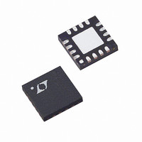
LTC4555EUD Linear Technology, LTC4555EUD Datasheet - Page 4

LTC4555EUD
Manufacturer Part Number
LTC4555EUD
Description
IC SIM PWR SUP/LVL TRNSLTR 16QFN
Manufacturer
Linear Technology
Datasheet
1.LTC4555EUD.pdf
(8 pages)
Specifications of LTC4555EUD
Function
Power Management, Signal Level Translation
Rf Type
Cellular
Secondary Attributes
SIM & Smart Card Interface
Package / Case
16-WFQFN Exposed Pad
Lead Free Status / RoHS Status
Contains lead / RoHS non-compliant
Available stocks
Company
Part Number
Manufacturer
Quantity
Price
Company:
Part Number:
LTC4555EUD
Manufacturer:
LT
Quantity:
10 000
Part Number:
LTC4555EUD
Manufacturer:
LT
Quantity:
20 000
Company:
Part Number:
LTC4555EUD#PBF
Manufacturer:
LT
Quantity:
33
Company:
Part Number:
LTC4555EUD#TRPBF
Manufacturer:
ZETEX
Quantity:
500
Part Number:
LTC4555EUD#TRPBF
Manufacturer:
ADI/亚德诺
Quantity:
20 000
LTC4555
TYPICAL PERFORMANCE CHARACTERISTICS
PIN FUNCTIONS
SHDN (Pin 1): Controller Driven Shutdown Pin. This pin
should be high (DV
activate a low current shutdown mode.
V
= 1.8V while driving this pin to DV
DV
Pins (C
is disabled. This pin should be bypassed with a 0.1μF
ceramic capacitor close to the pin.
NC (Pins 4, 6, 12, 16): No Connect.
V
3V and 6V for normal operation. V
reduces to <1μA in shutdown. This pin should be bypassed
with a 0.1μF ceramic capacitor close to the pin.
V
needs to be connected close to the V
tion. This pin is discharged to GND during shutdown.
I/O (Pin 8): SIM-Side Data I/O. The SIM card output must
be on an open-drain driver capable of sourcing >1mA.
4
SEL
BAT
CC
CC
(Pin 7): SIM Card V
(Pin 2): V
(Pin 5): V
(Pin 3): Supply Voltage for the Controller Side I/O
IN
, R
IN
, DATA). When below 1.1V, the V
CC
CC
Voltage Select Pin. A low level selects V
170
150
130
110
Supply Input. This pin can be between
90
70
50
–40
CC
V
CC
) for normal operation and low to
CC
–20
Short-Circuit Current
Supply. A 1μF low ESR capacitor
0
TEMPERATURE (°C)
20
CC
CC
BAT
40
pin for stable opera-
selects V
quiescent current
60
80
CC
CC
4555 G01
= 3V.
100
supply
CC
RST (Pin 9): Reset Output Pin for the SIM Card.
GND (Pin 10): Ground for the SIM and Controller. Proper
grounding and bypassing is required to meet 14kV ESD
specifi cations.
CLK (Pin 11): Clock Output Pin for the SIM Card. This
pin is pulled to ground during shutdown. Fast rising and
falling edges necessitate careful board layout for the CLK
node.
C
R
DATA (Pin 15): Controller Side Data I/O. This pin is used
for bidirectional data transfer. The controller output must
be an open-drain confi guration. The open-drain output
must be capable of sinking greater than 1mA.
Exposed Pad (Pin 17): GND. Must be soldered to PCB.
IN
IN
(Pin 13): Clock Input from the Controller.
(Pin 14): Reset Input from the Controller.
22
20
18
16
14
12
10
2.5
I
BAT
3.0
vs V
T
A
= 85°C
BAT
3.5
T
V
A
CC
= 25°C
T
4.0
V
= 3V
A
BAT
= 85°C
T
4.5
(V)
A
= –40°C
V
T
CC
A
= 25°C
5.0
= 1.8V
T
A
= –40°C
5.5
4555 G02
6.0
4555fb


