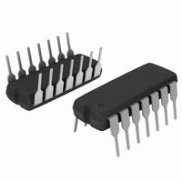
MC1496BPG ON Semiconductor, MC1496BPG Datasheet - Page 10

MC1496BPG
Manufacturer Part Number
MC1496BPG
Description
IC MODULATOR/DEMODULATOR 14-DIP
Manufacturer
ON Semiconductor
Datasheet
1.MC1496PG.pdf
(14 pages)
Specifications of MC1496BPG
Function
Modulator/Demodulator
Frequency
300MHz
Rf Type
FM
Package / Case
14-DIP (0.300", 7.62mm)
Maximum Operating Temperature
+ 125 C
Maximum Power Dissipation
33 mW (Typ)
Minimum Operating Temperature
- 40 C
Modulation Type
Balanced
Mounting Style
Through Hole
Supply Current
0.005 A
Supply Voltage Range
30V
Rf Ic Case Style
DIP
No. Of Pins
14
Operating Temperature Range
-40°C To +125°C
Digital Ic Case Style
DIP
Ic Function
Balanced Modulator / Demodulator
Rohs Compliant
Yes
Lead Free Status / RoHS Status
Lead free / RoHS Compliant
be introduced with or without modulation, provided its level
is sufficiently high to saturate the upper quad differential
amplifier. If the carrier signal is modulated, a 300 mVrms
input level is recommended.
Doubly Balanced Mixer
with either broadband or tuned narrow band input and output
networks.
port with a recommended amplitude of 100 mVrms.
tuned output.
Frequency Doubler
introducing the same frequency at both input ports.
Carrier Input
60 mVrms
Modulating
Signal Input
300 mVrms
Carrier
Null
Carrier
Modulating
The MC1496 may be used as a doubly balanced mixer
The local oscillator signal is introduced at the carrier input
Figure 29 shows a mixer with a broadband input and a
The MC1496 will operate as a frequency doubler by
Input
Signal
Input
50 k
V
V
C
S
0.1 mF
25 mF
15 V
750
−
10 mF
15 V
1.0 k
1.0 k
10 k
+
+
Carrier Adjust
50 k
10 k
Figure 27. AM Modulator Circuit
51
0.1 mF
750
0.1 mF
Figure 25. Balanced Modulator
820
(12 Vdc Single Supply)
51
100
51
0.1 mF
10
100
+
51
8
1
4
25 mF
15 V
1.0 k
10
8
1
4
MC1496
14
−
2
2
1.0 k
14
1.3 k
MC1496
V
−8.0 Vdc
R
EE
e
1.0 k
3
5
15 6.8 k
3.0 k
6
12
3
5
10 k
TYPICAL APPLICATIONS
3.9 k
6
12
R
L
3.0 k
http://onsemi.com
V
12 Vdc
0.1 mF
CC
V
12 Vdc
CC
−V
+V
3.9 k
DSB
Output
R
o
o
L
10
Carrier Input
300 mVrms
SSB Input
Modulating
and a tuned output very high frequency (VHF) doubler,
respectively.
Phase Detection and FM Detection
input signals are introduced at both inputs. When both inputs
are at the same frequency the MC1496 will deliver an output
which is a function of the phase difference between the two
input signals.
detector principle. A tuned circuit is added at one of the
inputs to cause the two input signals to vary in phase as a
function of frequency. The MC1496 will then provide an
output which is a function of the input signal frequency.
Carrier
Input
Signal
1.0 k
Input
Figures 30 and 31 show a broadband frequency doubler
The MC1496 will function as a phase detector. High−level
An FM detector may be constructed by using the phase
V
V
Figure 26. Balanced Modulator−Demodulator
C
S
0.1 mF
10 k
0.1 mF
0.1 mF
1.0 k
1.0 k
R1
Carrier Null
820
Figure 28. Product Detector
50 k
1.0 k
51
51
10 k
(12 Vdc Single Supply)
10
8
1
4
0.1
mF
0.1 mF
51
MC1496
14
2
0.1 mF
100
51
1.0 k
1.3 k
10
8
1
4
3
14
2
5
3.0 k
6
12
MC1496
V
−8.0 Vdc
R
10 k
EE
e
1.0 k
I5
V
12 Vdc
CC
3
0.005
mF
0.005
mF
5
6.8 k
1.0 k
3.0 k
3.9 k
12
6
R
L
1.0 mF
0.005
mF
R
L
V
12 Vd
q 10
Outp
CC
R
3.9
AF
L
−
+


