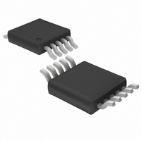
LTC1957-2EMS#TR Linear Technology, LTC1957-2EMS#TR Datasheet - Page 6

LTC1957-2EMS#TR
Manufacturer Part Number
LTC1957-2EMS#TR
Description
IC RF PWR CONTROLLR DUAL 10-MSOP
Manufacturer
Linear Technology
Datasheet
1.LTC1957-1EMS8.pdf
(16 pages)
Specifications of LTC1957-2EMS#TR
Rf Type
Cellular, GSM, GPRS, PCS, Wireless Modem, TDMA
Frequency
850MHz ~ 2GHz
Features
Dual Output
Package / Case
10-MSOP, Micro10™, 10-uMAX, 10-uSOP
Operating Supply Voltage (typ)
3.3/5V
Operating Supply Voltage (min)
2.7V
Operating Supply Voltage (max)
6V
Operating Temp Range
0C to 70C
Operating Temperature Classification
Commercial
Mounting
Surface Mount
Pin Count
10
Lead Free Status / RoHS Status
Contains lead / RoHS non-compliant
Other names
LTC1957-2EMSTR
Available stocks
Company
Part Number
Manufacturer
Quantity
Price
APPLICATIONS
LTC1957-1/LTC1957-2
Forward
The LTC1957 is an improved version of the LTC1757A.
The Schottky diode detector dynamic range has been
extended to over 40dB. The start voltage accuracy has
been improved to 17%. The autozero hold time has been
increased for applications requiring transmit times of
several hundred milliseconds. The PCTL input filter band-
width has been reduced to 350kHz for improved rejection
of DAC noise as well as smoother ramp shaping.
Operation
The LTC1957-2 dual band RF power control amplifier
integrates several functions to provide RF power control
over frequencies ranging from 850MHz to 2GHz. The
device also prevents damage to the RF power amplifier
due to overvoltage or overcurrent conditions. These func-
tions include an internally compensated power control,
amplifier to control the RF output power, an autozero
section to cancel internal and external voltage offsets, a
sense amplifier with an internal sense resistor to limit the
maximum RF power amplifier current, an RF Schottky
diode peak detector and amplifier to convert the RF feed-
back signal to DC, a V
sion, a bandgap reference, a thermal shutdown circuit and
a multiplexer to switch the control amplifier output to
either V
Band Selection
The LTC1957-2 is designed for dual band operation. The
BSEL pin will select output V
V
a 900MHz channel and V
BSEL must be established before the part is enabled. The
LTC1957-1 can be used to drive a single RF channel or
dual channel with integral multiplexer.
6
PCB
when high. For example, V
PCA
or V
PCB
U
.
PCA/B
INFORMATION
PCB
U
overvoltage clamp, compres-
a 1.8GHz/1.9GHz channel.
PCA
PCA
when low and output
could be used to drive
W
U
Control Amplifier
The control amplifier supplies the power control voltage to
the RF power amplifier. A portion (typically – 19dB for low
frequencies and –14dB for high frequencies) of the RF
output voltage is sampled, via a directional coupler, to
close the gain control loop. When a DAC voltage is applied
to PCTL, the amplifier quickly servos V
until the detected feedback voltage applied to the RF pin
matches the voltage at PCTL. This feedback loop provides
accurate RF power control. V
driving a 5.5mA load current and 100pF load capacitor.
RF Detector
The internal RF Schottky diode peak detector and ampli-
fier converts the RF feedback voltage from the directional
coupler to a low frequency voltage. This voltage is com-
pared to the DAC voltage at the PCTL pin by the control
amplifier to close the RF power control loop. The RF pin
input resistance is typically 200
range of this pin is 850MHz to 2000MHz. The detector
demonstrates excellent efficiency and linearity over a
wide range of input power. The Schottky detector is biased
at about 60 A and drives an on-chip peak detector capaci-
tor of 28pF.
Autozero
An autozero system is included to improve power pro-
gramming accuracy over temperature. This section can-
cels internal offsets associated with the Schottky diode
detector and control amplifier. External offsets associated
with the DAC driving the PCTL pin are also cancelled.
Offset drift due to temperature is cancelled between each
burst. The maximum offset allowed at the DAC output is
limited to 400mV. Autozeroing is performed when the
part is in autozero mode (SHDN = high, TXEN = low).
When the part is enabled (TXEN = high, SHDN = high) the
autozero capacitors are held and the V
connected to the control amplifier output. The hold droop
voltage of typically < 1 V/ms provides for accurate offset
PCA
or V
PCA
and the frequency
PCB
PCA
or V
are capable of
or V
PCB
PCB
positive
pin is


