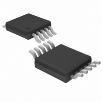
LTC4403-2EMS Linear Technology, LTC4403-2EMS Datasheet

LTC4403-2EMS
Specifications of LTC4403-2EMS
Available stocks
Related parts for LTC4403-2EMS
LTC4403-2EMS Summary of contents
Page 1
... RF power amplifiers operating in the 300MHz to 2.4GHz range. The LTC4403-2 has two outputs to control dual T PA modules with two control inputs. An internal sample and hold circuit enables the LTC4403 used with AM modulation via the carrier or PA supply. The input voltage range is optimized for operation from a single lithium-ion cell or 3 NiMH ...
Page 2
... PCTL LOAD LOAD = 2V High PCTL HOLD High to Hold Switch Opening HOLD = 2. 2. 3.6V HOLD IN ORDER PART TOP VIEW NUMBER BSEL LTC4403-2EMS 8 V HOLD 7 SHDN 6 PCTL MS PART MARKING MS PACKAGE = 125 C, = 160 C/W JA LTXJ unless otherwise noted. IN MIN TYP MAX 2 ...
Page 3
... RF INPUT POWER (dBm) 4403 G02 V (Pin 3): (LTC4403-2 Only) Power Control Voltage should PCB IN Output. This pin drives an external RF power amplifier power control pin. The maximum load capacitance is 100pF. The output is capable of rail-to-rail swings at low load currents. Selected when BSEL is high. ...
Page 4
... V (Pin 7/8): Asserted high prior to AM modulation, HOLD opens control loop and holds voltage at V EDGE modulation. BSEL (Pin 9): (LTC4403-2 Only) Selects V and V PCB resistor to ground. RF (Pin 8/10): Coupled RF Feedback Voltage . This input is referenced to V 2400MHz. This pin has an internal 250 termination, an ...
Page 5
... PCB PCA an 850MHz/900MHz channel and V channel. BSEL must be established before the part is enabled. The LTC4403-1 can be used to drive a single RF channel or dual channel with integral multiplexer. Control Amplifier The control amplifier supplies the power control voltage to the RF power amplifier. A portion (typically – 19dB for low frequencies and – ...
Page 6
... RF output signal is produced. The LTC4403-X V outputs must quickly rise to this threshold voltage in order to meet the power/time profile. To reduce this time, the LTC4403-X starts at 450mV. However, at very low power levels the PCTL input signal is small, and the V outputs may take several microseconds to reach the RF power amplifier threshold voltage ...
Page 7
... SHDN 11 s MINIMUM, ALLOWS TIME FOR AUTOZERO TO SETTLE Figure 1. LTC4403 Ramp Timing Demo Board The LTC4403-X demo board is available upon request. The demo board has a 900MHz and an 1800MHz RF channel and V controlled by the LTC4403-X. Timing signals HOLD for SHDN are generated on the board using a 13MHz crystal oscillator reference ...
Page 8
... VPCA loop configuration accounts for the nonlinear detector gain that is dependent on RF input voltage and frequency. The LTC4403-X unity gain bandwidth specified in the data sheet assumes that the net voltage gain contributed by the RF power amplifier and coupler network is unity. The bandwidth is calculated by measuring the rise time be- tween 10% and 90% of the voltage change at V for a small step in voltage applied to PCTL ...
Page 9
... In no event will Linear Technology be liable for special, collat- eral, incidental or consequential damages in connection with or arising out of the use of this model. It should be remembered that models are a simplification of the actual circuit. LTC4403-1/LTC4403-2 4403f 9 ...
Page 10
... PCTL **Open loop connections, comment-out EFB, VIN and VPCTL****** VPCTL PCTL VRF ******Add AC statement and print statement as required*** .AC DEC 50 10 1E7 *****for PSPICE only***** .OP .PROBE ************************* .END Figure 6. LTC4403-X Low Frequency AC SPICE Model ND3 ND4 GX1 GX2 RX1 + + 1E6 GM GM ND5 – ...
Page 11
... DETAIL “A” 0.254 (.010) 0 – 6 TYP 0.53 0.152 (.021 .006) 1.10 (.043) DETAIL “A” MAX SEATING PLANE 0.17 – 0.27 (.007 – .011) 0.50 TYP (.0197) BSC LTC4403-1/LTC4403-2 68 33pF HOLD 6 SHDN 5 DAC 4403 TA03 3.00 0.102 (.118 .004) 0.86 (NOTE 3) (.034) ...
Page 12
... Direct Conversion Quadrature Demodulator LT5516 Direct Conversion Quadrature Demodulator LT5522 High Linearity Downconvert Mixer LTC5532 Precision 7GHz RF Power Detector Linear Technology Corporation 12 1630 McCarthy Blvd., Milpitas, CA 95035-7417 (408) 432-1900 FAX: (408) 434-0507 Single Band Cellular Telephone Transmitter LTC4403 Li-Ion PCA HOLD ...


