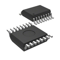
MICRF213AYQS Micrel Inc, MICRF213AYQS Datasheet - Page 7

MICRF213AYQS
Manufacturer Part Number
MICRF213AYQS
Description
IC RX 3.3V 300-350 MHZ 16-QSOP
Manufacturer
Micrel Inc
Datasheet
1.MICRF213AYQS.pdf
(16 pages)
Specifications of MICRF213AYQS
Operating Temperature
-40°C ~ 105°C
Frequency
300MHz ~ 350MHz
Sensitivity
-110dBm
Data Rate - Maximum
7.2 kbps
Modulation Or Protocol
AM, OOK
Applications
ISM, Garage Door Openers, RKE
Current - Receiving
3.9mA
Data Interface
PCB, Surface Mount
Antenna Connector
PCB, Surface Mount
Voltage - Supply
3 V ~ 3.6 V
Package / Case
16-QSOP
Receiving Current
3.9mA
Data Rate
7.2Kbps
Modulation Type
ASK, OOK
Frequency Range
300MHz To 350MHz
Rf Ic Case Style
QSOP
No. Of Pins
16
Supply Voltage Range
3V To 3.6V
Sensitivity Dbm
-110dBm
Rohs Compliant
Yes
Operating Temperature (min)
-40C
Operating Temperature (max)
105C
Operating Temperature Classification
Industrial
Operating Supply Voltage (typ)
3.3V
Operating Supply Voltage (max)
3.6V
Lead Free Status / RoHS Status
Lead free / RoHS Compliant
Features
-
Memory Size
-
Lead Free Status / Rohs Status
Compliant
Other names
576-1649-5
Available stocks
Company
Part Number
Manufacturer
Quantity
Price
Company:
Part Number:
MICRF213AYQS
Manufacturer:
MICREL
Quantity:
600
Part Number:
MICRF213AYQS
Manufacturer:
MICR
Quantity:
20 000
Detector and Programmable Low-Pass Filter
The demodulation starts with the detector removing the
carrier from the IF signal. Post detection, the signal
becomes base band information. The programmable
low-pass filter further enhances the base band
information. There are four programmable low-pass filter
BW settings: 1180Hz, 2360Hz, 4270Hz, 9400Hz for
315MHz operation. Low pass filter BW will vary with RF
Operating Frequency. Filter BW values can be easily
calculated by direct scaling. See the equation below for
the filter BW calculation:
BW
It is very important to choose filter setting that best fits
the intended data rate as this will minimize data
distortion.
Demod BW is set at 9700Hz @ 315MHz as default
(assuming both SEL0 and SEL1 pins are floating). The
low pass filter can be hardware set by external pins
SEL0 and SEL1.
Slicer, Slicing Level and Squelch
The signal, prior to slicer, is still linear demodulated AM.
Data slicer converts this signal into digital “1”s and “0”s
by comparing with the threshold voltage built up on the
CTH capacitor. This threshold is determined by
detecting the positive and negative peaks of the data
signal and storing the mean value. Slicing threshold
default is 50%. After the slicer, the signal becomes
digital OOK data.
During long periods of “0”s or no data period at all,
threshold voltage on the CTH capacitor may be very
low. Large random noise spikes during this time may
cause erroneous “1”s at DO pin. Squelch pin when pull
down low will suppress these errors.
AGC Comparator
The AGC comparator monitors the signal amplitude
from the output of the programmable low-pass filter.
When the output signal is less than 750mV threshold,
Micrel, Inc.
May 2007
Operating Freq
SEL0
0
1
0
1
Table 1. Demodulation BW Selection
= BW
SEL1
0
0
1
1
@315MHz
Demod BW (@ 315MHz)
1180Hz
2360Hz
4270Hz
9400Hz
×
⎛
⎜
⎝
Operating
- default
315
Freq
(MHz)
⎞
⎟
⎠
7
1.5µA current is then sourced into the external CAGC
capacitor. When the output signal is greater than
750mV, a 15µA current sink discharges the CAGC
capacitor. The voltage, developed on the CAGC
capacitor, acts to adjust the gain of the mixer and the IF
amplifier to compensate for RF input signal level
variation.
Reference Control
There are two components in Reference and Control
sub-block: 1) Reference Oscillator and, 2) Control Logic
through parallel Inputs: SEL0, SEL1, SHDN.
Reference Oscillator
RO2
The reference oscillator in the MICRF213 (reference
Figure 2) uses a basic Colpitts crystal oscillator
configuration with a MOS transconductor to provide
negative resistance. All capacitors shown in the figure
are integrated inside MICRF213. R01 and R02 are
external pins of MICRF213. The user only need connect
the reference oscillation crystal.
Reference oscillator crystal frequency can be calculated
thus as:
For 315MHz, F
To operate the MICRF213 with minimum offset, crystal
frequencies should be specified with 10pF loading
capacitance.
RO1
C
C
0
1
1
F
REFOSC
Figure 2. Reference Oscillator Circuit
Startup
Circuit
REFOSC
M4
= F
RF
/(32 + 1.1/12)
= 9.81563 MHz.
Normally on
R
C
C
1
C1
C2
M2
M1
gm
R
V
2
BIAS
M3
I
M9999-052307-A
BIAS
(408) 944-0800
MICRF213


