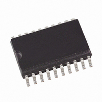
ATA5743P6-TKSY Atmel, ATA5743P6-TKSY Datasheet - Page 5

ATA5743P6-TKSY
Manufacturer Part Number
ATA5743P6-TKSY
Description
IC RCVR ASK/FSK 600KHZ 20SSOP
Manufacturer
Atmel
Datasheet
1.ATA5743P3-TGQY.pdf
(43 pages)
Specifications of ATA5743P6-TKSY
Frequency
300MHz ~ 450MHz
Sensitivity
-110dBm
Data Rate - Maximum
10 kBaud
Modulation Or Protocol
ASK, FSK
Applications
RKE, Telemetering, Security Technology
Current - Receiving
7.5mA
Data Interface
PCB, Surface Mount
Antenna Connector
PCB, Surface Mount
Voltage - Supply
4.5 V ~ 5.5 V
Operating Temperature
-40°C ~ 105°C
Package / Case
20-SOIC (0.300", 7.50mm Width)
Operating Frequency (max)
450000kHz
Operating Temperature (min)
-40C
Operating Temperature (max)
105C
Operating Temperature Classification
Industrial
Product Depth (mm)
4.4mm
Operating Supply Voltage (min)
4.5V
Operating Supply Voltage (typ)
5V
Operating Supply Voltage (max)
5.5V
Lead Free Status / RoHS Status
Lead free / RoHS Compliant
Features
-
Memory Size
-
Lead Free Status / Rohs Status
Compliant
4. RF Front-end
4839B–RKE–08/05
The RF front-end of the receiver is a heterodyne configuration that converts the input signal into
a 1 MHz IF signal. As seen in
Amplifier), an LO (Local Oscillator), a mixer, and an RF amplifier.
The LO generates the carrier frequency for the mixer via a PLL synthesizer. The XTO (crystal
oscillator) generates the reference frequency f
erates the drive voltage frequency f
and is then divided by 64. The divided frequency is compared to f
detector. The current output of the phase frequency detector is connected to a passive loop filter
and thereby generates the control voltage V
is controlled in a way that f
the following formula: f
The XTO is a one-pin oscillator that operates at the series resonance of the quartz crystal. As
demonstrated in
value of that capacitor is recommended by the crystal supplier. The value of C
mized for the individual board layout to achieve the exact value of f
designing the system in terms of receiving bandwidth, the accuracy of the crystal and the XTO
must be considered.
Figure 4-1.
The passive loop filter connected to pin LF is designed for a loop bandwidth of B
This value for B
the appropriate loop filter components to achieve the desired loop bandwidth. If the filter compo-
nents are changed for any reason, please note that the maximum capacitive load at pin LF is
limited. If the capacitive load is exceeded, a bit check may no longer be possible since f
not settle in time before the bit check starts to evaluate the incoming data stream. Self polling
will also not work in that case.
f
mula: f
To determine f
frequency is f
is tuned by the crystal frequency f
f
LO
LO
. This relation is dependent on the logic level at pin MODE.
is determined by the RF input frequency f
LO
= f
RF
IF
LO
PLL Peripherals
- f
= 1 MHz. To achieve a good accuracy of the filter’s corner frequencies, the filter
Loop
, the construction of the IF filter must be considered at this point. The nominal IF
IF
Figure
exhibits the best possible noise performance of the LO.
XTO
4-1, the crystal should be connected to GND via a capacitor C
= f
LO
/64 is equal to f
LO
Figure 3-2 on page
/64.
LFGND
LFVCC
DVCC
XTO
LF
XTO
LO
. This means that there is a fixed relation between f
for the mixer. f
V
V
S
S
XTO
LF
RF
C9
XTO
for the VCO. By means of that configuration, V
. If f
R1
and the IF frequency f
4, the front-end consists of an LNA (Low-Noise
. The VCO (voltage-controlled oscillator) gen-
LO
is determined, f
C10
LO
C
L
is dependent on the voltage at pin LF,
C9 = 4.7 nF
C10 = 1 nF
R1 = 820
XTO
XTO
XTO
IF
and hereby of f
by the phase frequency
can be calculated using
using the following for-
Figure 4-1
ATA5743
L
should be opti-
Loop
= 100 kHz.
LO
. When
LO
shows
L
IF
. The
can-
and
LF
5


