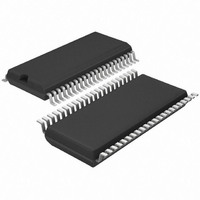
T4260-ILSH Atmel, T4260-ILSH Datasheet - Page 4

T4260-ILSH
Manufacturer Part Number
T4260-ILSH
Description
IC AM/FM FRONT END W/PLL 44SSOP
Manufacturer
Atmel
Datasheet
1.T4260-ILQH.pdf
(34 pages)
Specifications of T4260-ILSH
Frequency
AM, FM
Modulation Or Protocol
AM, FM
Applications
AM/FM Radio Receiver
Current - Receiving
85mA
Data Interface
PCB, Surface Mount
Antenna Connector
PCB, Surface Mount
Voltage - Supply
8 V ~ 10 V
Operating Temperature
-40°C ~ 85°C
Package / Case
44-SSOP
Lead Free Status / RoHS Status
Lead free / RoHS Compliant
Features
-
Sensitivity
-
Memory Size
-
Data Rate - Maximum
-
Table 2-1.
3. Functional Description
4
Pin
21
22
23
24
25
26
27
28
29
30
31
32
33
34
35
36
37
38
39
40
41
42
43
44
T4260
Pin Description (Continued)
RFAGCFM
REFFREQ
RFAGCA1
MXAMOB
IFAGCFM
MXAMOA
MXFMOA
MXFMOB
OSCBUF
IFAGCA1
The T4260 implements an AM up-conversion reception path from the RF input signal to the IF
output signal. A VCO and an LO prescaler for AM are integrated to generate the LO frequency to
the AM mixer. The FM reception path generates the same LO frequency from the RF input sig-
nal by a down-conversion to the IF output. The IF A/D output is designed for digital signal
processing. The IF can be chosen in the range of 10 MHz to 25 MHz. Automatic gain control
(AGC) circuits are implemented to control the preamplifier stages in the AM and FM reception
paths.
For improved performance, the PLL has an integrated special 2-bit shift fractional logic with spu-
rious suppression that enables fast frequency changes in AM and FM mode by a low step
frequency (f
alignment via a microcontroller.
For a double-tuner concept, external voltage can be applied at the input of the DACs, the inter-
nal PLL can switched off and the OSC buffer (output) can also be used as input.
Several register bits (bit 0 to bit 145) are used to control the circuit’s operation and to adapt cer-
tain circuit parameters to the specific application. The control bits are organized in four 8-bit, four
16-bit and three 24-bit registers that can be programmed by the 3-wire bus protocol. The bus
protocol and the bit-to-register mapping is described in
page
GNDPLL
IFOUTB
Symbol
IFOUTA
IFINAM
IFINFM
VRPLL
IFREF
OSCB
GNDT
DATA
CLK
VRT
VST
EN
10. The meaning of the control bits is mentioned in the following sections.
PDF
). In addition, two programmable DACs (Digital to Analog Converter) support the
Function
Oscillator base
Oscillator buffer output/input
3-wire bus Enable
3-wire bus Clock
3-wire bus Data
PLL reference voltage
PLL reference frequency
PLL ground
IF output B
IF output A
FM IF-AGC filter
AM IF-AGC filter 1
RF FM-AGC filter
IF amplifier reference input
IF amplifier AM input
IF amplifier FM input
Tuner reference voltage
Tuner ground
AM mixer output B
AM mixer output A
Tuner supply voltage
RF AM-AGC filter 1
FM mixer output A
FM mixer output B
Section 8. “3-wire Bus Description” on
4528N–AUDR–11/09


