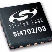
SI4702-B16-GM Silicon Laboratories Inc, SI4702-B16-GM Datasheet - Page 4

SI4702-B16-GM
Manufacturer Part Number
SI4702-B16-GM
Description
IC FM RADIO TUNER 20QFN
Manufacturer
Silicon Laboratories Inc
Datasheet
1.SI4703-B17-EVB.pdf
(46 pages)
Specifications of SI4702-B16-GM
Frequency
76MHz ~ 108MHz
Sensitivity
-99dBm
Modulation Or Protocol
FM
Applications
Cellular, MP3, PDAs, Portable Radios
Current - Receiving
18mA
Data Interface
PCB, Surface Mount
Antenna Connector
PCB, Surface Mount
Voltage - Supply
2.7 V ~ 5.5 V
Operating Temperature
-20°C ~ 85°C
Package / Case
20-QFN
Lead Free Status / RoHS Status
Lead free / RoHS Compliant
Features
-
Memory Size
-
Data Rate - Maximum
-
Lead Free Status / RoHS Status
Lead free / RoHS Compliant, Lead free / RoHS Compliant
Other names
336-1333-1
Available stocks
Company
Part Number
Manufacturer
Quantity
Price
Company:
Part Number:
SI4702-B16-GM
Manufacturer:
Silicon Labs
Quantity:
135
Part Number:
SI4702-B16-GM
Manufacturer:
SILICONIX
Quantity:
20 000
Part Number:
SI4702-B16-GMR
Manufacturer:
SILICON LABS/èٹ¯ç§‘
Quantity:
20 000
Si4702/03-C19
1. Electrical Specifications
Table 1. Recommended Operating Conditions
Table 2. Absolute Maximum Ratings
4
Parameter
Digital Supply Voltage
Analog Supply Voltage
Interface Supply Voltage
Digital Power Supply Power-Up
Rise Time
Analog Power Supply Power-Up
Rise Time
Interface Power Supply Power-Up
Rise Time
Ambient Temperature
Note: All minimum and maximum specifications are guaranteed and apply across the recommended operating conditions.
Parameter
Digital Supply Voltage
Analog Supply Voltage
Interface Supply Voltage
Input Current
Input Voltage
Operating Temperature
Storage Temperature
RF Input Level
Notes:
1. Permanent device damage may occur if the above Absolute Maximum Ratings are exceeded. Functional operation
2. The Si4702/03-C19 device is a high-performance RF integrated circuit with an ESD rating of < 2 kV HBM. Handling
3. For input pins SCLK, SEN, SDIO, RST, RCLK, GPIO1, GPIO2, and GPIO3.
4. At RF input pins.
Typical values apply at V
otherwise stated.
should be restricted to the conditions as specified in the operational sections of this data sheet. Exposure beyond
recommended operating conditions for extended periods may affect device reliability.
and assembly of this device should only be done at ESD-protected workstations.
3
3
4
D
= V
A
= 3.3 V and 25 °C unless otherwise stated. Parameters are tested in production unless
Symbol
V
V
V
IORISE
DRISE
ARISE
V
V
V
T
1,2
IO
A
D
A
Symbol
T
T
V
V
V
V
I
STG
OP
IN
IO
IN
D
A
Rev. 1.1
Test Condition
–0.3 to (V
–0.5 to 5.8
–0.5 to 5.8
–0.5 to 3.9
–55 to 150
–40 to 95
Value
±10
0.4
Min
–20
2.7
2.7
1.5
10
10
10
IO
+ 0.3)
Typ
25
—
—
—
—
—
—
Max
5.5
5.5
3.6
85
—
—
—
Unit
V
mA
°C
°C
V
V
V
V
pK
Unit
µs
µs
µs
°C
V
V
V


