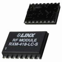
RXM-418-LC-S Linx Technologies Inc, RXM-418-LC-S Datasheet - Page 2

RXM-418-LC-S
Manufacturer Part Number
RXM-418-LC-S
Description
RECEIVER RF 418MHZ SMT
Manufacturer
Linx Technologies Inc
Series
LCr
Datasheet
1.RXM-315-LC-S.pdf
(9 pages)
Specifications of RXM-418-LC-S
Frequency
418MHz
Sensitivity
-95dBm
Data Rate - Maximum
5 kbps
Modulation Or Protocol
ASK, OOK
Applications
ISM, Garage Door Openers, RKE
Current - Receiving
5mA
Data Interface
PCB, Surface Mount
Antenna Connector
PCB, Surface Mount
Voltage - Supply
2.7 V ~ 4.2 V
Operating Temperature
-30°C ~ 70°C
Package / Case
Non-Standard SMD
Lead Free Status / RoHS Status
Contains lead / RoHS non-compliant
Features
-
Memory Size
-
PERFORMANCE DATA–RXM-***-LC
ABSOLUTE MAXIMUM RATINGS
Page 2
Parameters
RXM-315-LC-S
Operating Voltage
Current Continuous
Current in Sleep
Data Out Voltage
Data Out Voltage
Receive Frequency
Noise BW
Sensitivity @10
Baud Rate
Settling Time
ABOUT THESE MEASUREMENTS
w/Dropping Resistor
The performance parameters listed
below
operation at 25°C from a 3VDC.
Figure 1 at the right illustrates the
connections necessary for testing
and operation. It is recommended
that all ground pads be connected to
the groundplane. The pads marked
NC have no physical connection and
are designed only to add support.
Logic Low
Logic High
Supply voltage V
Operating temperature
Storage temperature
Soldering temperature
RF input, pin 16
Any input or output pin
*NOTE*
damage to the device. Furthermore, extended operation at these maximum
ratings may reduce the life of this device.
are
-5
BER
Exceeding any of the limits of this section may lead to permanent
based
CC
Designation
I
I
SLP
CC
on
(V
(V
V
V
V
V
V
F
CC
CC
CC
CC
OH
OH
OL
C
=3V)
module
=3V)
314.925
V
Min.
CC
100
2.7
4.7
4.0
2.7
-92
–
0
–
5
-0.3
-30°C
-45°C
Figure 1: Test/Basic Application Circuit
External
Resistor
-0.3
-0.3
-0.3
200
+225°C for 10 sec.
5VDC
Typical
315.0
700
280
5.0
3.4
-95
–
–
–
–
–
7
0 dBm
3VDC
to
to
to
to
to
315.075
(
Note 5)
5,000
Max.
-100
930
V
V
4.2
5.2
7.0
0.2
10
+70°C
+85°C
–
(SEE NOTES 3,4)
CC
CC
+4.2
+5.2
1
2
3
4
5
6
7
8
Vcc
NC
NC
NC
GND
VCC
PDN
NC
DATA
Units
mSec
VDC
VDC
VDC
VDC
VDC
MHz
dBm
kHz
mA
bps
µA
VDC
VDC
GND
ANT
NC
NC
NC
NC
NC
NC
Notes
16
15
14
13
12
11
10
9
–
3
–
–
–
–
4
–
–
1
_
2
Notes:
1.
2.
3.
4.
5.
Parameters
RXM-418-LC-S
Operating Voltage
Current Continuous
Current in Sleep
Data Out Voltage
Data Out Voltage
Receive Frequency
Noise BW
Sensitivity @10
Baud Rate
Settling Time
Parameters
RXM-433-LC-S
Operating Voltage
Current Continuous
Current in Sleep
Data Out Voltage
Data Out Voltage
Receive Frequency
Noise BW
Sensitivity @10
Baud Rate
Settling Time
For BER of 10
Time to valid data output.
*CRITICAL* In order to operate the device over this range it is necessary for a 200 resistor to be placed
in-line with VCC.
When operating from a 5 volt source it is important to consider that the output will swing to well less than
5 volts as a result of the required dropping resistor. Please verify that the minimum voltage will meet the
high threshold requirment of the device to which data is being sent.
Maximum output voltage measured after in-line dropping resistor.
w/Dropping Resistor
w/Dropping Resistor
Logic Low
Logic High
Logic High
Logic Low
-5
-5
-5
at 4800 baud. Sensitivity is affected by antenna SWR. See Figure 3.
BER
BER
Designation
I
Designation
I
I
I
SLP
SLP
CC
CC
(V
(V
(V
(V
V
V
V
V
V
V
V
V
V
V
F
F
CC
CC
CC
CC
CC
OL
OH
OH
CC
CC
CC
OL
OH
OH
C
C
=3V)
=3V)
=3V)
=3V)
433.845
V
417.925
V
CC
100
-92
2.7
4.0
Min.
Min.
CC
100
2.7
4.7
4.0
2.7
-92
4.7
–
0
2.7
–
5
-0.3
–
0
–
5
-0.3
433.92
Typical
Typical
700
280
-95
5.0
700
418
280
5.0
3.4
-95
–
–
–
–
7
3.4
–
–
–
–
7
–
–
418.075
433.995
(
(
Note 5)
5,000
Note 5)
5,000
Max.
Max.
-100
-100
930
930
V
V
V
V
4.2
5.2
7.0
0.2
4.2
5.2
7.0
0.2
10
10
–
–
CC
CC
CC
CC
Units
mSec
Units
mSec
VDC
VDC
VDC
VDC
VDC
MHz
dBm
VDC
VDC
VDC
VDC
VDC
MHz
dBm
kHz
bps
kHz
bps
mA
mA
µA
µA
Notes
Notes
Page 3
–
3
–
–
–
–
4
–
–
1
_
2
–
3
–
–
–
–
4
–
–
1
–
2


