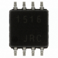
NJG1516R-TE1 NJR, NJG1516R-TE1 Datasheet - Page 13

NJG1516R-TE1
Manufacturer Part Number
NJG1516R-TE1
Description
IC MMIC SWITCH SPDT 8-VSP
Manufacturer
NJR
Series
-r
Datasheet
1.NJG1516R-TE1.pdf
(14 pages)
Specifications of NJG1516R-TE1
Rf Type
GSM
Frequency
1MHz ~ 3GHz
Features
SPDT
Package / Case
8-VSP
Lead Free Status / RoHS Status
Contains lead / RoHS non-compliant
Other names
NJG1516R-TE1TR
PRECAUTIONS
[1]The DC blocking capacitors have to be placed at RF terminal of P1, P2 and PC.
[2]Bypass capacitors (C4, C5) should be placed close to terminals of VCTL1, VCTL2 to reduce
[3]For good isolation, the GND terminal (3
[4] To avoid degradation of isolation or high power characteristics, please layout ground pattern
APPLICATION CIRCUIT
RECOMMENDED PCB DESIGN
stripline influence of RF characteristics.
plane of substrate, and through holes for GND should be placed near by the pin connection.
right under this IC.
Circuit losses including losses of
capacitors and connectors.
Frequency (GHz)
P2
0.8
1.0
1.5
1.8
2.0
2.5
VCTL2 (0V/3V)
VCTL1 (0V/3V)
VCTL2
PC
C4
C2
Loss (dB)
(TOP VIEW)
0.12
0.13
0.17
0.19
0.20
0.26
1pin
PC
C3
C3
C4
C5
C1
C5
1
2
3
4
rd
VCTL1
, 6
th
NJG1516R
, 7
th
pin) must be placed possibly close to ground
Freq(MHz)
PARTS LIST
PART ID
P1
C1~C3
C4, C5
8
5
7
6
PCB: FR-4, t=0.5mm
Capacitor: size 1005
Microstrip Line Width=1.0mm (Zo=50Ω)
PCB SIZE: 19.4 x 14mm
C2
C1
50~100
0.01uF
10pF
1
P2
P1
100~500
1000pF
10pF
NJG1516R
2
500~2000
56pF
10pF
- 13 -
3


