WISMC03BI Laird Technologies, WISMC03BI Datasheet - Page 7
WISMC03BI
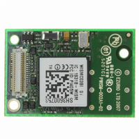
Manufacturer Part Number
WISMC03BI
Description
MODULE LAN 802.11B/G BISM
Manufacturer
Laird Technologies
Series
EZURiOr
Specifications of WISMC03BI
Frequency
2.4GHz
Data Rate - Maximum
1Mbps
Modulation Or Protocol
802.11 b/g
Applications
AMR, Automotive, ISM
Power - Output
15dBm
Sensitivity
-86dBm
Voltage - Supply
3.3 V ~ 5.5 V
Current - Transmitting
250mA
Data Interface
Connector, 50 Pin, DF-12
Memory Size
64Mbyte Flash, 16MByte SRAM
Antenna Connector
U.FL
Operating Temperature
-40°C ~ 85°C
Package / Case
Module
Wireless Frequency
2.412 GHz to 2.484 GHz
Interface Type
UART
Board Size
22.8 mm x 33.8 mm x 7.6 mm
Modulation
BPSK, CCK, DSSS, QPSK
Security
WEP 64/128, WPA-PSK, WPA2, TKIP, AES-CCMP
Lead Free Status / RoHS Status
Lead free / RoHS Compliant
Current - Receiving
-
Lead Free Status / Rohs Status
Lead free / RoHS Compliant


4.1
4.1.1
Absolute maximum ratings for supply voltage and voltages on digital and analogue pins of the Module
are listed below. Exceeding these values will cause permanent damage.
4.1.2
4.1.2.1
4.1.2.2
4.1.2.3
4.1.2.4
DSH_WISMC03_0v97 WISM 40 pin SLIP Data Sheet.doc
Parameter
Peak current of power supply
Voltage at digital pins
Voltage at VCC_5V pin
Signal Name
VCC_5V
GND
Signal Type
Input
Output
Signal Name
UART_TX
UART_RX
UART_CTS
UART_RTS
UART_DSR
UART_DTR
UART_RI
UART_DCD
Signal Name
GPIO 1 - 9
GPIO 10 – 13
ADC0, ADC1
Electrical Specifications
Absolute Maximum ratings
Recommended Operating Parameters
Power Supply
Signal Levels for Interface and GPIO
RS-232 Interface
General Purpose I/O and ADC
Pin No
28, 29, 31
11,15,18,30,36,38
Signal level
Pin No
Pin No
2,4,14,16,33,35,37, 39
10,12,6,8
1, 3
V
V
V
IH
IL
IH
max=0.8V
max=3.3V
21
25
19
23
10
12
min=2.1V
6
8
I/O
O
O
O
O
O
I
I
I
Signal level @ 0mA load
Comments
This pin must NOT be pulled low by external circuitry.
Used to place the module in Powersave 2 mode
Direction is programmable – default is Output
Direction is programmable – default is Output
Direction is programmable – default is Output
Min
3.3
-0.3
Voltage level
3.3V to 5.0V
V
V
OL
OH
I or O
I or O
I/O
max=0.2V
min=2.8V
I
Comments
There is no GPIO3
Shared with DSR, DTR, RI, DCD
Range 0 – 3.0V
© 2007-8 EZURiO Ltd
All VCC_5V pins should be connected
All six GND pins should be connected
Comments
I
Max
550
3.3
5
typ
= 250mA.
Signal level @ 4mA load
V
V
OL
OH
max=0.4V
min=2.6V
Unit
mA
V
V
Page 7
Related parts for WISMC03BI
Image
Part Number
Description
Manufacturer
Datasheet
Request
R

Part Number:
Description:
Bluetooth Serial Module Development Kit
Manufacturer:
Laird Technologies
Part Number:
Description:
BLUETOOTH MODULE DEVELOPMENT KIT
Manufacturer:
Laird Technologies
Part Number:
Description:
Bluetooth 2.0 AT Data Module, Internal Antenna Development Kit
Manufacturer:
Laird Technologies

Part Number:
Description:
BLUETOOTH EVAL BOARD BTM511
Manufacturer:
Laird Technologies
Datasheet:

Part Number:
Description:
Bluetooth / 802.15.1 Modules & Development Tools BLUETTH Multimed MODLE, No ANT DEVKIT
Manufacturer:
Laird Technologies
Datasheet:

Part Number:
Description:
DEV KIT PRM122
Manufacturer:
Laird Technologies
Datasheet:
Part Number:
Description:
DEV KIT PRM123
Manufacturer:
Laird Technologies
Datasheet:

Part Number:
Description:
KIT FOR PRM112
Manufacturer:
Laird Technologies
Datasheet:
Part Number:
Description:
DEV KIT PRM121
Manufacturer:
Laird Technologies
Datasheet:

Part Number:
Description:
KIT DEVELOPMENT FOR LT2510 U.FL
Manufacturer:
Laird Technologies
Datasheet:

Part Number:
Description:
CHOKE COMMON MODE 110 OHMS SMD
Manufacturer:
Laird Technologies
Datasheet: