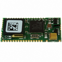
GS-BT2416C2.H STMicroelectronics, GS-BT2416C2.H Datasheet
GS-BT2416C2.H
Specifications of GS-BT2416C2.H
GS-BT2416C2.H


Related parts for GS-BT2416C2.H


GS-BT2416C2.H Summary of contents
Page 1
... CE Compliant IMQ Exp. Opinion 0081- AREF0017 – Safety EN60950-1 (2001) – EMC EN301 489 17V1.2.1 – Radio ES 300 328 V1.6 ■ FCC certified on GS-BT2416C2DB ( for a more exhaustive explanation , please refer to GS-BT2416C2DB Application Note ) ■ FCC ID: S9N16C2 ■ BQB qualified module BQB ID: B012535 ...
Page 2
... Contents Contents 1 Maximum ratings . . . . . . . . . . . . . . . . . . . . . . . . . . . . . . . . . . . . . . . . . . . . 3 1.1 Absolute maximum ratings . . . . . . . . . . . . . . . . . . . . . . . . . . . . . . . . . . . . . 3 1.2 Operating ranges . . . . . . . . . . . . . . . . . . . . . . . . . . . . . . . . . . . . . . . . . . . . 3 2 I/O specification . . . . . . . . . . . . . . . . . . . . . . . . . . . . . . . . . . . . . . . . . . . . . 4 3 Bluetooth section . . . . . . . . . . . . . . . . . . . . . . . . . . . . . . . . . . . . . . . . . . . 4 4 Block diagram . . . . . . . . . . . . . . . . . . . . . . . . . . . . . . . . . . . . . . . . . . . . . . 5 5 Pin settings . . . . . . . . . . . . . . . . . . . . . . . . . . . . . . . . . . . . . . . . . . . . . . . . 6 6 Mechanical dimensions . . . . . . . . . . . . . . . . . . . . . . . . . . . . . . . . . . . . . . 8 7 Revision history . . . . . . . . . . . . . . . . . . . . . . . . . . . . . . . . . . . . . . . . . . . . 9 2/10 GS-BT2416C2 ...
Page 3
... GS-BT2416C2 1 Maximum ratings 1.1 Absolute maximum ratings Operation of the module beyond these limits is not guaranteed. Sustained exposure to these limits will adversely affect device reliability. Table 1. Absolute maximum ratings Symbol V Module supply voltage DD V Input voltage on any digital pin IN T Storage temperature ...
Page 4
... Operation current RX mode 4/10 Parameter Conditions 3.13 V < 3.13 V < 3.13 V < load = pin drive capability Io load = pin drive capability Parameter Conditions 3.13V < 3.13V < 3.13V < GS-BT2416C2 Values Min Typ Max < 3.47 V 0.8 < 3. < 3.47 V 0.4 0. 0.15 Values Min Typ Max < 3.47V 0 < ...
Page 5
... GS-BT2416C2 4 Block diagram Figure 1. Block diagram UART USB PCM SPI I2C GPIO 32kHz 13MHz XTAL XTAL STA2416 STLC2150 Baseband Radio chip ARM7 proc Block diagram RF antenna Filter balun 5/10 ...
Page 6
... Pin settings 5 Pin settings Table 5. Pin description Pin N° Name 1 TDI 2 TMS 3 NTRST 4 TDO 5 TCK 6 INT1 7 I2C_dat 8 I2C_clk 9 PCM_CLK 10 PCM_SYNC 11 PCM_B 12 PCM_A 13 UART2_RXD 14 UART2_TXD 15 UART2_I1 16 UART2_02 17 SPI_FRM 18 SPI_CLK 19 SPI_TXD 20 SPI_RXD 21 USB_DN 22 USB_DP 23 RESET 24 BOOT 25 GPIO0 6/10 I/O Description JTAG pin JTAG pin ...
Page 7
... I/O General purpose I/O line I/O General purpose I/O line I/O General purpose I/O line I/O General purpose I/O line I/O General purpose I/O line -- Module supply voltage- Single 3.3V -- GND -- RF GND -- Antenna out -- RF GND Pin settings 7/10 ...
Page 8
... Mechanical dimensions 6 Mechanical dimensions Figure 2. Mechanical dimensions Figure 3. Land pattern and connection diagram 8/10 GS-BT2416C2 ...
Page 9
... GS-BT2416C2 7 Revision history Table 6. Document revision history Date 20-Dec-2006 28-Feb-2007 31-Aug-2007 Revision 1 First release 2 Typo Table 5: Pin description on page 6 Updates involved: Cover page, 3 page 6. Revision history Changes Table 4 on page 4, Table 5 on 9/10 ...
Page 10
... Australia - Belgium - Brazil - Canada - China - Czech Republic - Finland - France - Germany - Hong Kong - India - Israel - Italy - Japan - Malaysia - Malta - Morocco - Singapore - Spain - Sweden - Switzerland - United Kingdom - United States of America 10/10 Please Read Carefully: © 2007 STMicroelectronics - All rights reserved STMicroelectronics group of companies www.st.com GS-BT2416C2 ...