TRM-433-LT Linx Technologies Inc, TRM-433-LT Datasheet - Page 6
TRM-433-LT
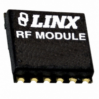
Manufacturer Part Number
TRM-433-LT
Description
TRANSCEIVER RF 433MHZ LT SERIES
Manufacturer
Linx Technologies Inc
Series
LTr
Datasheet
1.TRM-418-LT.pdf
(13 pages)
Specifications of TRM-433-LT
Frequency
433MHz
Data Rate - Maximum
10kbps
Modulation Or Protocol
AM, OOK
Applications
ISM, 2-way Paging, Robotics, Telemetry
Power - Output
10dBm
Sensitivity
-112dBm
Voltage - Supply
2.1 V ~ 3.6 V
Current - Receiving
6.1mA
Current - Transmitting
12mA
Data Interface
PCB, Surface Mount
Antenna Connector
PCB, Surface Mount
Operating Temperature
-40°C ~ 85°C
Package / Case
Surface Mount
Board Size
15.7 mm x 16 mm x 3.2 mm
Minimum Operating Temperature
- 40 C
Supply Voltage (min)
2.1 V
Product
RF Modules
Maximum Frequency
433.92 MHz
Supply Voltage (max)
3.6 V
Maximum Operating Temperature
+ 85 C
Lead Free Status / RoHS Status
Lead free / RoHS Compliant
Memory Size
-
Lead Free Status / Rohs Status
Lead free / RoHS Compliant


USING THE DATA LINE
Page 10
The CMOS-compatible DATA line is used for both the transmitter data and the
recovered receiver data. Its function is controlled by the state of the T/R SEL line,
so it will be an input when in transmit mode and an output when in receive mode.
The output is normally connected to a transcoder IC or a microprocessor for data
encoding and decoding.
It is important to note that the transceiver does not provide hysteresis or
squelching of the DATA line when in receive mode. This means that, in the
absence of a valid transmission or transitional data, the DATA line will switch
randomly. This is a result of the receiver sensitivity being below the noise floor
of the board. This noise can be handled in software by implementing a noise-
tolerant protocol as described in Linx Application Note AN-00160. If a software
solution is not appropriate, then the transceiver can be squelched.
Squelching will disable the DATA output when the RSSI voltage falls below a
reference level. This prevents low amplitude noise from causing the DATA line
to switch, reducing hash during times that the transmitter is off or during
transmitter steady-state times which exceed 15mS.
The voltage on the A REF line is the analog reference voltage that is used by the
tranceiver’s data circuit. The received signal must be higher than this voltage for
the DATA line to activate and must then fall lower than this output for the DATA
line to deactivate. This voltage will dynamically follow the midpoint of the
received signal’s voltage. There is always about 30mVp-p noise riding on the
signal’s voltage. During times with no carrier or during transmitter steady-state
times exceeding 15mS, the reference voltage will reach a point where the noise
will cause the output to switch randomly.
To squelch the DATA line,
an offset can be added to
the
connecting a resistor to
Vcc. This offset will keep
the reference voltage above
the noise, and quiet the
DATA line. Typical resistor
values are between 1MΩ
and 10MΩ.
Squelching the output will
reduce the sensitivity of the
receiver and, therefore, the range of the system. For this reason, the squelch
threshold will normally be set as low as possible, but the designer can make the
compromise between noise level on the DATA line and range of the system. It
should also be noted that squelching will cause some bit stretching and
contracting, which could affect PWM-based protocols.
It is important to recognize that in many actual use environments, ambient noise
and interference may enter the receiver at levels well above the squelch
threshold. For this reason, it is always recommended that the product’s protocol
be structured to allow for the possibility of hashing, even when an external
squelch circuit is employed.
A
REF
line
by
Figure 20: Sensitivity Degradation vs. Squelch Resistor
-102
-104
-106
-108
-110
-112
-114
-116
-118
O pen 10
Higher Sensitivity, More Hash
9.1
8.2
7.5
6.8
6.2
5.6
5.1
Resistor Value (MΩ)
4.7
4.3
3.9
3.6
3.3
Lower Sensitivity, Less Hash
3
2.7
2.2
2
1.6
1.3
1
USING LADJ
TRANSFERRING DATA
The Level Adjust (LADJ) line allows the transceiver’s output power to be easily
adjusted for range control, lower power consumption, or to meet legal
requirements. This is done by placing a resistor between V
value of the resistor determines the output power level. When LADJ is connected
to V
shows a graph of the output power vs. LADJ resistance.
This line is very useful during FCC testing to compensate for antenna gain or
other product-specific issues that may cause the output power to exceed legal
limits. A variable resistor can be temporarily used so that the test lab can
precisely adjust the output power to the maximum level allowed by law. The
variable resistor’s value can be noted and a fixed resistor substituted for final
testing. Even in designs where attenuation is not anticipated, it is a good idea to
place a resistor pad connected to LADJ and V
For more sophisticated designs, LADJ can also be controlled by a DAC or digital
potentiometer to allow precise and digitally-variable output power control.
Once a reliable RF link has been established, the challenge becomes how to
effectively transfer data across it. While a properly designed RF link provides
reliable data transfer under most conditions, there are still distinct differences
from a wired link that must be addressed. The LT Series is intended to be as
transparent as possible and does not incorporate internal encoding or decoding,
so a user has tremendous flexibility in how data is handled.
If you want to transfer simple control or status signals, such as button presses or
switch closures, and your product does not have a microprocessor on board (or
you simply wish to avoid protocol development), consider using an encoder and
decoder, or a transcoder IC set. These chips are available from a wide range of
manufacturers, including Linx. These chips take care of all encoding and
decoding functions, and generally provide a number of data pins to which
switches can be directly connected. In addition, address bits are usually provided
for security and to allow the addressing of multiple units independently. These
ICs are an excellent way to bring basic remote control / status products to market
quickly and inexpensively. Additionally, it is a simple task to interface with
inexpensive microprocessors, or one of many IR, remote control, or modem ICs.
It is always important to separate the types of transmissions that are technically
possible from those that are legally allowable in the country of intended
operation. Linx Application Notes AN-00125, AN-00128, and AN-00140 should
be reviewed, along with Part 15, Section 231 of the Code of Federal Regulations
for further details regarding acceptable transmission content in the U.S. All of
these
www.linxtechnologies.com.
Another area of consideration is that the data structure can affect the output
power level. The FCC allows output power in the 260 to 470MHz band to be
averaged over a 100mS time frame. Because OOK modulation activates the
carrier for a ‘1’ and deactivates the carrier for a ‘0’, a data stream that sends
more ‘0’s will have a lower average output power over 100mS. This allows the
instantaneous output power to be increased, thus extending range.
CC
, the output power and current consumption will be the highest. Figure 3
documents
can
be
downloaded
CC
so that it can be used if needed.
from
our
CC
and LADJ. The
website
Page 11
at
Related parts for TRM-433-LT
Image
Part Number
Description
Manufacturer
Datasheet
Request
R

Part Number:
Description:
TRANSCEIVER RF 418MHZ LT SERIES
Manufacturer:
Linx Technologies Inc
Datasheet:

Part Number:
Description:
TRANSCEIVER RF 315MHZ LT SERIES
Manufacturer:
Linx Technologies Inc
Datasheet:

Part Number:
Description:
TRM RNG TUBE N INS 250 KCMIL 1/2
Manufacturer:
Panduit Corp
Datasheet:
Part Number:
Description:
TRM RNG TUBE N INS 250 KCMIL 3/8
Manufacturer:
Panduit Corp
Datasheet:
Part Number:
Description:
TRM RNG TUBE N INS 250 KCMIL7/16
Manufacturer:
Panduit Corp
Datasheet:
Part Number:
Description:
TRM RNG TUBE N INS 250 KCMIL5/16
Manufacturer:
Panduit Corp
Datasheet:
Part Number:
Description:
TRM RNG TUBE N INS 250 KCMIL 3/8
Manufacturer:
Panduit Corp
Datasheet:
Part Number:
Description:
TRM RNG TUBE N INS 250 KCMIL5/16
Manufacturer:
Panduit Corp
Datasheet:
Part Number:
Description:
TRM RNG TUBE N INS 250 KCMIL7/16
Manufacturer:
Panduit Corp
Datasheet:

Part Number:
Description:
HOLDER BATTERY 20MM COIN CR2032
Manufacturer:
Linx Technologies Inc
Datasheet:

Part Number:
Description:
MODULE USB LOW SPEED
Manufacturer:
Linx Technologies Inc
Datasheet:

Part Number:
Description:
IC TRANSCODER MT BI-DIR 20-SSOP
Manufacturer:
Linx Technologies Inc
Datasheet:

Part Number:
Description:
IC ENCODER LOW SECURITY 8DIP
Manufacturer:
Linx Technologies Inc
Datasheet:

Part Number:
Description:
IC DECODER MS SERIES 20-SSOP
Manufacturer:
Linx Technologies Inc
Datasheet:
Part Number:
Description:
IC ENCODER MS SERIES 20-SSOP
Manufacturer:
Linx Technologies Inc
Datasheet: