TR3005 RFM, TR3005 Datasheet - Page 10
TR3005
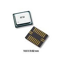
Manufacturer Part Number
TR3005
Description
ASH TR 115.2 KBPS 403.5 MHZ
Manufacturer
RFM
Series
TRr
Datasheet
1.TR3005.pdf
(12 pages)
Specifications of TR3005
Frequency
403.55MHz
Data Rate - Maximum
115.2kbps
Modulation Or Protocol
ASK, OOK
Applications
ISM
Power - Output
0dBm
Sensitivity
-109dBm
Voltage - Supply
2.2 V ~ 3.7 V
Current - Receiving
3.8mA
Current - Transmitting
7.5mA
Data Interface
PCB, Surface Mount
Antenna Connector
PCB, Surface Mount
Operating Temperature
-10°C ~ 55°C
Package / Case
SM-20H
Wireless Frequency
403.5 MHz
Operating Supply Voltage
2.5 V, 3.3 V
Maximum Operating Temperature
+ 85 C
Mounting Style
SMD/SMT
Maximum Data Rate
115.2 Kbps
Minimum Operating Temperature
- 10 C
Modulation
OOK/ASK
Lead Free Status / RoHS Status
Lead free by exemption / RoHS compliant by exemption
Memory Size
-
Lead Free Status / Rohs Status
Lead free / RoHS Compliant
Other names
583-1090-2


Pin
10
11
12
13
14
8
9
LPFADJ
TXMOD
PRATE
THLD2
THLD1
GND2
Name
RREF
The trans mit ter RF out put volt age is pro por tional to the in put cur rent to this pin. A se ries re sis tor is used to ad just
the peak trans mit ter out put volt age. 0 dBm out put power re quires about 250 µA of in put cur rent. In the ASK mode,
min i mum out put power oc curs when the mod u la tion driver sinks about 10 µA of cur rent from this pin. In the OOK
mode, in put sig nals less than 220 mV com pletely turn the trans mit ter os cil la tor off. In ternally, this pin ap pears to
be a di ode in se ries with a small re sis tor. Peak trans mit ter out put power P
mately:
A ±5% re sis tor value is rec om mended. In the OOK mode, this pin is usu ally driven with a logic-level data in put
(unshaped data pulses). OOK mod u la tion is prac ti cal for data pulses of 30 µs or lon ger. In the ASK mode, this pin
ac cepts an a log mod u la tion (shaped or unshaped data pulses). ASK mod u la tion is prac ti cal for data pulses 8.7 µs
or lon ger. The re sis tor driv ing this pin must be low in the re ceive and power-down (sleep) modes. Please re fer to
the ASH Trans ceiver De signer’s Guide for ad di tional in for ma tion on mod u la tion tech niques.
This pin is the re ceiver low-pass fil ter band width ad just. The fil ter band width is set by a re sis tor R
pin and ground. The re sis tor value can range from 330 K to 820 ohms, pro vid ing a fil ter 3 dB band width f
4.5 kHz to 1.8 MHz. The re sis tor value is de ter mined by:
A ±5% re sis tor should be used to set the fil ter band width. This will pro vide a 3 dB fil ter band width be tween f
and 1.3* f
equiripple phase re sponse. The peak drive cur rent avail able from RXDATA in creases in pro por tion to the fil ter
band width set ting.
GND2 is an IC ground pin. It should be connected to GND1 by a short, low in duc tance trace.
RREF is the ex ter nal ref er ence re sis tor pin. A 100 K ref er ence re sis tor is con nected be tween this pin and ground.
A ±1% re sis tor tol er ance is rec om mended. It is im por tant to keep the to tal ca pac i tance be tween ground, Vcc and
this node to less than 5 pF to main tain cur rent source sta bil ity. If THLD1 and/or THDL2 are con nected to RREF
through re sis tor val ues less that 1.5 K, their node ca pac i tance must be added to the RREF node ca pac i tance and
the to tal should not ex ceed 5 pF.
THLD2 is the “dB-below-peak” data slicer (DS2) thresh old ad just pin. The thresh old is set by a 0 to 200 K re sis tor
R
tec tor value (in creases dif fer ence) from 0 to 120 mV. For most ap pli ca tions, this thresh old should be set at 6 dB
be low peak, or 60 mV for a 50%-50% RF am pli fier duty cy cle. The value of the THLD2 re sis tor is given by:
A ±1% re sis tor tol er ance is rec om mended for the THLD2 re sis tor. Leaving the THLD2 pin open dis ables the
dB-below-peak data slicer op er a tion.
The THLD1 pin sets the thresh old for the stan dard data slicer (DS1) through a re sis tor R
old is in creased by in creas ing the re sis tor value. Con necting this pin di rectly to RREF pro vides zero thresh old.
The value of the re sis tor de pends on whether THLD2 is used. For the case that THLD2 is not used, the ac cept -
able range for the re sis tor is 0 to 100 K, pro vid ing a THLD1 range of 0 to 90 mV. The re sis tor value is given by:
For the case that THLD2 is used, the ac cept able range for the THLD1 re sis tor is 0 to 200 K, again pro vid ing a
THLD1 range of 0 to 90 mV. The re sis tor value is given by:
A ±1% re sis tor tol er ance is rec om mended for the THLD1 re sis tor. Note that a non-zero DS1 thresh old is re quired
for proper AGC op er a tion.
The in ter val be tween the fall ing edge of an ON pulse to the first RF am pli fier and the ris ing edge of the next ON
pulse to the first RF am pli fier t
justed be tween 0.1 and 5 µs with a re sis tor in the range of 51 K to 2000 K. The value of R
A ±5% re sis tor value is rec om mended. When the PWIDTH pin is con nected to Vcc through a 1 M re sis tor, the RF
am pli fi ers op er ate at a nom i nal 50%-50% duty cy cle, fa cil i tat ing high data rate op er a tion. In this case, the pe riod
t
to 1.1 µs us ing a re sis tor of 11 K to 220 K. In this case the value of R
A ±5% re sis tor value should also be used in this case. Please re fer to the ASH Trans ceiver De signer’s Guide for
ad di tional am pli fier duty cy cle in for ma tion. It is im por tant to keep the to tal ca pac i tance be tween ground, Vcc and
this pin to less than 5 pF to main tain sta bil ity.
PRC
TH2
from start-to-start of ON pulses to the first RF am pli fier is con trolled by the PRATE re sis tor over a range of 0.1
be tween this pin and RREF. In creasing the value of the re sis tor de creases the thresh old be low the peak de -
P
R
R
R
R
R
R
LPF
O
LPF
TH2
TH1
TH1
PR
PR
= 16*(I
with vari a tions in sup ply volt age, tem per a ture, etc. The fil ter pro vides a three-pole, 0.05 de gree
= 404* t
= 198* t
= 1445/ f
= 1.67*V, where R
= 1.11*V, where R
= 2.22*V, where R
TXM
PRI
PRC
)
2
LPF
, where P
+ 10.5, where t
- 8.51, where t
, where R
PRI
TH2
TH1
TH1
is set by a re sis tor R
O
is in mW, and the peak mod u la tion cur rent I
LPF
is in kilohms and the thresh old V is in mV
is in kilohms and the thresh old V is in mV
is in kilohms and the thresh old V is in mV
is in kilohms, and f
PRI
PRC
is in µs, and R
10
is in µs and R
Description
PR
be tween this pin and ground. The in ter val t
PR
PR
LPF
is in kilohms
is in kilohms
is in kHz
PR
is given by:
O
for a 3 Vdc sup ply volt age is ap prox i -
TXM
is in mA
TH1
PR
to RREF. The thresh -
is given by:
LPF
PRI
be tween this
can be ad -
LPF
LPF
from
Related parts for TR3005
Image
Part Number
Description
Manufacturer
Datasheet
Request
R

Part Number:
Description:
TRANSCEIVER RF 916MHZ 1/2-DUPLEX
Manufacturer:
Linx Technologies Inc
Datasheet:
Part Number:
Description:
TRANSCEIVER RF 916MHZ 1/2-DUPLEX
Manufacturer:
Linx Technologies Inc
Datasheet:
Part Number:
Description:
TXCVR RF 900MHZ 1/2-DUPLEX 180CH
Manufacturer:
Linx Technologies Inc
Part Number:
Description:
TRANSCEIVER RF 916MHZ 20PIN SMD
Manufacturer:
Linx Technologies Inc
Datasheet:

Part Number:
Description:
ASH TR 115.2 KBPS 433.92 MHZ
Manufacturer:
RFM
Datasheet:

Part Number:
Description:
ASH TR 115.2 KBPS 916.5 MHZ
Manufacturer:
RFM
Datasheet:

Part Number:
Description:
ASH TR 115.2 KBPS 433.92 MHZ
Manufacturer:
RFM
Datasheet:
Part Number:
Description:
ASH TR 115.2 KBPS 916.5 MHZ
Manufacturer:
RFM
Datasheet:

Part Number:
Description:
ASH RX 115.2 KBPS 433.92 MHZ
Manufacturer:
RFM
Datasheet:

Part Number:
Description:
RFIC TRANCEIVER MULTI-CHANNEL FS
Manufacturer:
RFM
Datasheet:
Part Number:
Description:
10-Terminal Ceramic Surface-Mount Case 7 x 5 mm Nominal Footprint
Manufacturer:
RFM [RF Monolithics, Inc]
Datasheet:
Part Number:
Description:
QUAD-BAND GSM850/GSM/DCS/PCS POWER AMP MODULE
Manufacturer:
RFM [RF Monolithics, Inc]
Datasheet:
Part Number:
Description:
402 to 405 MHz Medical Band Front-end Filter
Manufacturer:
RFM [RF Monolithics, Inc]
Datasheet:
Part Number:
Description:
674.03 MHz SAW Resonator
Manufacturer:
RFM [RF Monolithics, Inc]
Datasheet: