DM1810-916MB RFM, DM1810-916MB Datasheet - Page 3
DM1810-916MB
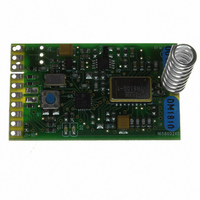
Manufacturer Part Number
DM1810-916MB
Description
DM1810 916.5 MHZ MESH MODULE BAS
Manufacturer
RFM
Series
DM1810r
Datasheet
1.DM1810-916MB.pdf
(4 pages)
Specifications of DM1810-916MB
Frequency
916.5MHz
Data Rate - Maximum
4.8kbps
Modulation Or Protocol
OOK
Applications
Wireless Mesh Networks
Power - Output
10mW
Voltage - Supply
2.6 V ~ 10 V
Current - Receiving
5.5mA
Current - Transmitting
15.75mA
Data Interface
Pads for Pins
Antenna Connector
On-Board, Spring
Operating Temperature
-40°C ~ 85°C
Package / Case
Module
Lead Free Status / RoHS Status
Lead free / RoHS Compliant
Sensitivity
-
Memory Size
-
Lead Free Status / Rohs Status
Lead free / RoHS Compliant
Other names
583-1035


Canadian Department of Communications Industry
Notice - IC: 4492A-DM1810A
This apparatus complies with Health Canada’s Safety
Code 6 / IC RSS 210. To prevent radio interference to
the licensed service, this device is intended to be
operated indoors and away from windows to provide
maximum shielding. Equipment (or its transmit an-
tenna) that is installed outdoors may be subject to
licensing.
DM1810-916MB I/O Pad Descriptions
www.RFM.com E-mail: info@rfm.com
©2008 by RF Monolithics, Inc.
J1-10
J1-1
J1-2
J1-3
J1-4
J1-5
J1-6
J1-7
J1-8
J1-9
J3-1
J3-2
J3-3
J4-1
J4-2
Pin
CAUTION: Electrostatic Sensitive Device. Observe precautions when handling.
SERIAL RX
SERIAL TX
VOUT
Name
BIND
GND
GND
GND
GND
ANT
VIN
D1
D2
-
-
-
This pad is a signal and power supply ground.
This is the power supply input pad. The allowed input voltage range is 2.6 to 10 V.
VOUT tracks 50 to 100 mV below VIN when VIN is in the range of 2.6 to 3.1 V. When VIN is in the range of 3.1
to 10 V, VOUT is regulated at 3.0 Vdc. Up to 10 mA can be supplied from this pad for powering external circuits
such as thermistor-resistor networks. External circuitry must not impress more than 10 mV
lated output voltage.
This pad is connected to a logic input on the microcontroller, and is configured with a weak pull-up. When this
pin is momentarily grounded to J1-1 or J1-10, the module is placed into the bind mode, allowing this module to
be associated with other modules to form a network.
This pad is unused in base station operation. Leave this pad electrically unconnected.
This pad is unused in base station operation. Leave this pad electrically unconnected.
This pad is unused in base station operation. Leave this pad electrically unconnected.
This pad is connected to the module’s serial data input (USART). Data to this pin is received at 9.6 kb/s, using
8 data bits, no parity, and one stop bit. The input voltage range on this pad is 0 to VOUT. Applying a voltage
outside of this range may damage the module.
This pad is connected to the module’s serial data output (USART) through a 1 kilohm resistor, which provides
short-circuit protection. Data from this pad is sent at 9.6 kb/s, using 8 data bits, no parity, and one stop bit.
This pad is a signal and power supply ground.
This pad is a ground for the antenna port.
This pad is the antenna port.
This pad is a ground for the antenna port.
This pad is the LED 1 signal.
This pad is the LED 2 signal.
ICES-003
This digital apparatus does not exceed the Class B
limits for radio noise emissions from digital apparatus
as set out in the radio interference regulations of In-
dustry Canada.
Le present appareil numerique n’emet pas de bruits
radioelectriques depassant les limites applicables aux
appareils numeriques de Classe B prescrites dans le
reglement sur le brouillage radioelectrique edicte par
Industrie Canada.
Description
DM1810-916MB - 4/17/08
p-p
ripple on the regu-
Page 3 of 4
Related parts for DM1810-916MB
Image
Part Number
Description
Manufacturer
Datasheet
Request
R

Part Number:
Description:
DM1810 916.5 MHZ MESH MODULE FIE
Manufacturer:
RFM
Datasheet:

Part Number:
Description:
DM1810 433.92 MHZ MESH MODULE BA
Manufacturer:
RFM
Datasheet:

Part Number:
Description:
DM1810 433.92 MHZ MESH MODULE FI
Manufacturer:
RFM
Datasheet:

Part Number:
Description:
DM1810 433.92 MHZ MESH MODULE RO
Manufacturer:
RFM
Datasheet:

Part Number:
Description:
DM1810 916.5 MHZ MESH MODULE ROU
Manufacturer:
RFM
Datasheet:

Part Number:
Description:
DM1810 916.5 MHZ DEVELOPMENT KIT
Manufacturer:
RFM
Datasheet:

Part Number:
Description:
DM1810 433.92 MHZ DEVELOPMENT KI
Manufacturer:
RFM
Datasheet:

Part Number:
Description:
DM1810 433.92 MHZ QUICK KIT, BAS
Manufacturer:
RFM
Datasheet:

Part Number:
Description:
DM1810 916.5 MHZ QUICK KIT, BASE
Manufacturer:
RFM
Datasheet:

Part Number:
Description:
RF Modules & Development Tools DM1810 Network Routr 433.92 MHz Vert Mnt
Manufacturer:
RFM


Part Number:
Description:
10-Terminal Ceramic Surface-Mount Case 7 x 5 mm Nominal Footprint
Manufacturer:
RFM [RF Monolithics, Inc]
Datasheet:
Part Number:
Description:
QUAD-BAND GSM850/GSM/DCS/PCS POWER AMP MODULE
Manufacturer:
RFM [RF Monolithics, Inc]
Datasheet:
Part Number:
Description:
402 to 405 MHz Medical Band Front-end Filter
Manufacturer:
RFM [RF Monolithics, Inc]
Datasheet:
Part Number:
Description:
674.03 MHz SAW Resonator
Manufacturer:
RFM [RF Monolithics, Inc]
Datasheet: