DP1283C433 Semtech, DP1283C433 Datasheet - Page 9
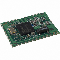
DP1283C433
Manufacturer Part Number
DP1283C433
Description
MODULE DROP IN FOR XE1283 433MHZ
Manufacturer
Semtech
Datasheet
1.DP1283C433.pdf
(12 pages)
Specifications of DP1283C433
Frequency
433MHz
Data Rate - Maximum
153.2kbps
Applications
ISM
Power - Output
11dBm
Sensitivity
-111dBm
Voltage - Supply
2.4 V ~ 3.6 V
Current - Receiving
14mA
Current - Transmitting
40mA
Data Interface
PCB, Surface Mount
Antenna Connector
PCB, Surface Mount
Operating Temperature
-40°C ~ 85°C
Package / Case
Module
Lead Free Status / RoHS Status
Contains lead / RoHS non-compliant
Memory Size
-
Modulation Or Protocol
-


4.1
The drop-in module DP1283 can be programmed using the 3-wire bus or the pin SWITCH. This section describes the
switching sequence from Mode 1 to Mode 2.
4.2
In most applications, the CPU clock will be given by the on-chip RC oscillator combined with the pre-mounted 32 kHz
oscillator for calibration (connected between pins XIN and XOUT).
For specific applications where an external clock is required, the 32 kHz crystal has to be removed and the external
CPU clock signal can be injected on XIN pin.
4.3
In both cases the Antenna switch embedded on the DP1283 is by default driven by the microcontroller through PB4 and
PB5.
However, it is possible to drive the antenna switch externally via RX and TX pins. In this case, two resistors have to be
moved as explained on the following table:
© Semtech 2005
Switching sequence using the 3-wire bus
Switch_ext = 0 (Bit 3, Address 00010)
Switching sequence using pad SWITCH
Switch_ext = 1 (Bit 3, Address 00010)
STANDARD SEQUENCE FOR SWITCHING BETWEEN RECEIVER AND TRANSMITTER
MICROCONTROLLER CLOCK
ANTENNA SWITCH
R4, R5
R1, R3
Truth Table:
Switch driven internally (PB4 & PB5)
PB4
1
0
0 Ω
NC
PB5
0
1
Receiver mode
Transmitter mode
9
Switch driven externally (RX & TX pins)
NC
0Ω
www.semtech.com
DP1283
Related parts for DP1283C433
Image
Part Number
Description
Manufacturer
Datasheet
Request
R

Part Number:
Description:
EVALUATION BOARD
Manufacturer:
Semtech
Datasheet:
Part Number:
Description:
EVALUATION BOARD
Manufacturer:
Semtech
Datasheet:
Part Number:
Description:
VOLTAGE SUPPRESSOR, TRANSIENT SEMTECH
Manufacturer:
Semtech
Datasheet:

Part Number:
Description:
HIGH VOLTAGE CAPACITORS MONOLITHIC CERAMIC TYPE
Manufacturer:
Semtech Corporation
Datasheet:
Part Number:
Description:
EZ1084CM5.0 AMP POSITIVE VOLTAGE REGULATOR
Manufacturer:
Semtech Corporation
Datasheet:
Part Number:
Description:
3.0 AMP LOW DROPOUT POSITIVE VOLTAGE REGULATORS
Manufacturer:
Semtech Corporation
Datasheet:
Part Number:
Description:
Manufacturer:
Semtech Corporation
Datasheet:
Part Number:
Description:
RailClamp Low Capacitance TVS Diode Array
Manufacturer:
Semtech Corporation
Datasheet:
Part Number:
Description:
Manufacturer:
Semtech Corporation
Datasheet:
Part Number:
Description:
Manufacturer:
Semtech Corporation
Datasheet:
Part Number:
Description:
Manufacturer:
Semtech Corporation
Datasheet:
Part Number:
Description:
Manufacturer:
Semtech Corporation
Datasheet: