FA38SA50LC Vishay, FA38SA50LC Datasheet
FA38SA50LC
Specifications of FA38SA50LC
VS-FA38SA50LC
VS-FA38SA50LC
VSFA38SA50LC
VSFA38SA50LC
Available stocks


Related parts for FA38SA50LC

FA38SA50LC Summary of contents
Page 1
... Operating Junction and J T Storage Temperature Range STG V Insulation Withstand Voltage (AC-RMS) ISO Mounting torque, M4 srew Thermal Resistance Parameter R Junction-to-Case JC R Case-to-Sink, Flat, Greased Surface CS www.irf.com FA38SA50LC HEXFET The low thermal @ 10V GS @ 10V GS Typ. ––– 0. 91615B ® Power MOSFET V = 500V ...
Page 2
... FA38SA50LC Electrical Characteristics @ T Parameter V Drain-to-Source Breakdown Voltage (BR)DSS Breakdown Voltage Temp. Coefficient (BR)DSS J R Static Drain-to-Source On-Resistance DS(on) V Gate Threshold Voltage GS(th) g Forward Transconductance fs I Drain-to-Source Leakage Current DSS Gate-to-Source Forward Leakage I GSS Gate-to-Source Reverse Leakage Q Total Gate Charge g Q Gate-to-Source Charge ...
Page 3
... TOP BOTTOM 100 Fig 2. Typical Output Characteristics 3 2.5 2.0 1.5 1.0 0.5 = 50V 0.0 -60 -40 - Fig 4. Normalized On-Resistance FA38SA50LC VGS 15V 10V 8.0V 7.0V 6.0V 5.5V 5.0V 4.5V 4.5V 20µs PULSE WIDTH ° 150 Drain-to-Source Voltage (V) DS 38A V = 10V GS ...
Page 4
... FA38SA50LC 16000 1MHz iss 14000 rss oss ds gd 12000 10000 C iss 8000 6000 C oss 4000 C rss 2000 Drain-to-Source Voltage (V) DS Fig 5. Typical Capacitance Vs. Drain-to-Source Voltage 1000 100 T = 150 C ° ° 0.1 0.2 0.4 0.6 0.8 1.0 V ,Source-to-Drain Voltage (V) SD Fig 7. Typical Source-Drain Diode ...
Page 5
... Fig 11. Maximum Effective Transient Thermal Impedance, Junction-to-Case www.irf.com 10V Pulse Width Duty Factor Fig 10a. Switching Time Test Circuit d(on) Fig 10b. Switching Time Waveforms Notes: 1. Duty factor Peak 0.001 0. Rectangular Pulse Duration (sec) 1 FA38SA50LC D.U. µ d(off thJC C 0 ...
Page 6
... FA38SA50LC . Fig 12a. Unclamped Inductive Test Circuit Fig 12b. Unclamped Inductive Waveforms 6 1200 1000 D RIV E R 800 + - 600 A 400 200 Starting T , Junction Temperature ( C) Fig 12c. Maximum Avalanche Energy I D TOP 17A 24A BOTTOM 38A 50 75 100 125 ° J Vs. Drain Current www ...
Page 7
... Driver same type as D.U.T. I controlled by Duty Factor "D" SD D.U.T. - Device Under Test Period D = P.W. Waveform SD Body Diode Forward Current di/dt Waveform DS Diode Recovery dv/dt Body Diode Forward Drop Ripple for Logic Level Devices Fig 13. For N-Channel HEXFETS FA38SA50LC + + P.W. Period V =10V * ...
Page 8
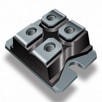
... FA38SA50LC SOT-227 Package Details . Tube QUANTITY PER SREW AND W ASHE R IN CLUDED WORLD HEADQUARTERS: 233 Kansas St., El Segundo, California 90245, Tel: (310) 322 3331 IR GREAT BRITAIN: Hurst Green, Oxted, Surrey RH8 9BB, UK Tel 1883 732020 IR GERMANY: Saalburgstrasse 157, 61350 Bad Homburg Tel 6172 96590 IR FAR EAST: K& ...