FSB50825US Fairchild Semiconductor, FSB50825US Datasheet - Page 3
FSB50825US
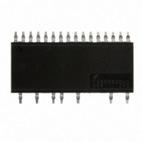
Manufacturer Part Number
FSB50825US
Description
IC POWER MOD SPM 250V 4A SPM23BD
Manufacturer
Fairchild Semiconductor
Series
SPM™r
Type
FETr
Datasheet
1.FSB50825US.pdf
(8 pages)
Specifications of FSB50825US
Configuration
3 Phase
Current
4A
Voltage
250V
Voltage - Isolation
1500Vrms
Package / Case
SPM23BD
Lead Free Status / RoHS Status
Lead free / RoHS Compliant
Other names
FSB50825USTR
Available stocks
Company
Part Number
Manufacturer
Quantity
Price


FSB50825US Rev. A
Electrical Characteristics
Inverter Part
Control Part
Note:
1. For the measurement point of case temperature T
2. BV
3. t
4. The peak current and voltage of each FRFET during the switching operation should be included in the safe operating area (SOA). Please see Figure 5 for the RBSOA test cir-
Package Marking & Ordering Information
Device Marking
Symbol
Symbol
ΔBV
RBSOA
effect of the stray inductance so that V
field applcations due to the effect of different printed circuit boards and wirings. Please see Figure 4 for the switching time definition with the switching test circuit of Figure 5.
cuit that is same as the switching test circuit.
R
UV
UV
BV
UV
UV
ON
E
I
I
I
DS(on)
V
t
E
ΔT
QCC
FSB50825US
DSS
t
QBS
V
DSS
OFF
V
I
ON
OFF
I
t
and t
ON
IH
SD
CCD
CCR
IL
DSS
rr
BSD
BSR
IH
DSS
IL
J
is the absolute maximum voltage rating between drain and source terminal of each FRFET inside SPM
OFF
/
include the propagation delay time of the internal drive IC. Listed values are measured at the laboratory test condition, and they can be different according to the
Drain-Source Breakdown
Voltage
Breakdown Voltage Tem-
perature Coefficient
Zero Gate Voltage
Drain Current
Static Drain-Source
On-Resistance
Drain-Source Diode
Forward Voltage
Switching Times
Reverse-bias Safe Oper-
ating Area
Quiescent V
Quiescent V
Low-side Undervoltage
Protection (Figure 6)
High-side Undervoltage
Protection (Figure 7)
ON Threshold Voltage
OFF Threshold Voltage
Input Bias Current
(Each HVIC Unless Otherwise Specified)
(Each FRFET Unless Otherwise Specified)
Parameter
Parameter
CC
BS
FSB50825US
Current
Current
Device
DS
should not exceed BV
C
, please refer to Figure 3 in page 4.
(T
V
I
V
V
V
V
V
Inductive load L=3mH
High- and low-side FRFET switching
(Note 3)
V
T
High- and low-side FRFET switching (Note 4)
V
V
V
V
V
V
Logic High Level
Logic Low Level
V
V
D
J
IN
IN
CC
CC
PN
IN
PN
CC
BS
CC
CC
BS
BS
IN
IN
J
= 250μA, Referenced to 25°C
= 150°C
= 0V, I
= 0V, V
= 25°C, V
= 0V ↔ 5V
=15V, V
= 5V
= 0V
=15V, V
= 150V, V
= 200V, V
Undervoltage Protection Detection Level
Undervoltage Protection Reset Level
= V
= V
Undervoltage Protection Detection Level
Undervoltage Protection Reset Level
BS
BS
DSS
D
Package
SPM23-BD
DS
= 15V, V
= 15V, V
= 250μA (Note 2)
IN
in any case.
IN
CC
=0V
= 250V
=0V
CC
CC
=V
= V
= V
BS
Conditions
IN
IN
Conditions
Applied between V
Applied between V
V
Applied between IN and COM
Applied between IN and COM
BS
BS
=15V Unless Otherwise Specified)
B(V)
= 5V, I
= 0V, I
3
= 15V, I
= 15V, I
-V, V
D
D
B(W)
= 2.0A
= -2.0A
D
D
Reel Size
= 2.0A
= I
-W
330mm
DP
, V
CC
B(U)
DS
and COM
-U,
®
=BV
. V
PN
DSS
should be sufficiently less than this value considering the
Packing Type
,
Tape & reel
Min
Min Typ Max Units
250
7.4
8.0
7.4
8.0
3.0
-
-
-
-
-
-
-
-
-
-
-
-
-
-
1050
Typ Max Units
0.31
450
140
100
8.0
8.9
8.0
8.9
10
Full Square
-
-
-
-
-
5
-
-
-
-
160
100
0.45
9.4
9.8
9.4
9.8
0.8
250
20
1.2
2
-
-
-
-
-
-
-
-
Quantity
www.fairchildsemi.com
450
μA
μA
μA
μA
V
V
V
V
V
V
μA
ns
ns
ns
μJ
μJ
Ω
V
V
V
Related parts for FSB50825US
Image
Part Number
Description
Manufacturer
Datasheet
Request
R

Part Number:
Description:
Fairchild Semiconductor [IGBT MODULE]
Manufacturer:
Fairchild Semiconductor
Datasheet:

Part Number:
Description:
Discrete Semiconductor Modules
Manufacturer:
Fairchild Semiconductor
Part Number:
Description:
Discrete Semiconductor Modules
Manufacturer:
Fairchild Semiconductor
Part Number:
Description:
This N-Channel MOSFET is produced using Fairchild Semiconductor’s advanced Power Trench® process
Manufacturer:
Fairchild Semiconductor
Datasheet:
Part Number:
Description:
This N-Channel MOSFET is produced using Fairchild Semiconductor’s advanced Power Trench® process
Manufacturer:
Fairchild Semiconductor
Datasheet:
Part Number:
Description:
This N-Channel MOSFET is produced using Fairchild Semiconductor’s advanced PowerTrench® process
Manufacturer:
Fairchild Semiconductor
Datasheet:
Part Number:
Description:
This N-Channel MOSFET is produced using Fairchild Semiconductor’s advanced PowerTrench® process
Manufacturer:
Fairchild Semiconductor
Datasheet:
Part Number:
Description:
This N-Channel MOSFET is produced using Fairchild Semiconductor’s advanced Power Trench® process
Manufacturer:
Fairchild Semiconductor
Datasheet:
Part Number:
Description:
This N-Channel logic Level MOSFETs are produced using Fairchild Semiconductor‘s advanced Power Trench® process that has been special tailored to minimize the on-state resistance and yet maintain superior switching performance
Manufacturer:
Fairchild Semiconductor
Datasheet:
Part Number:
Description:
This N-Channel MOSFET is produced using Fairchild Semiconductor’s advanced Power Trench® process
Manufacturer:
Fairchild Semiconductor
Datasheet:
Part Number:
Description:
This N-Channel SyncFET™ is produced using Fairchild Semiconductor’s advanced PowerTrench® process
Manufacturer:
Fairchild Semiconductor
Datasheet:
Part Number:
Description:
This N-Channel SyncFET™ is produced using Fairchild Semiconductor’s advanced PowerTrench® process
Manufacturer:
Fairchild Semiconductor
Datasheet:
Part Number:
Description:
This N-Channel SyncFET™ is produced using Fairchild Semiconductor’s advanced PowerTrench® process
Manufacturer:
Fairchild Semiconductor
Datasheet:
Part Number:
Description:
This N-Channel logic Level MOSFETs are produced using Fairchild Semiconductor‘s advanced Power Trench® process that has been special tailored to minimize the on-state resistance and yet maintain superior switching performance
Manufacturer:
Fairchild Semiconductor
Datasheet:
Part Number:
Description:
This N-Channel MOSFET is produced using Fairchild Semiconductor’s advanced Power Trench® process that has been especially tailored to minimize the on-state resistance and yet maintain superior switching performance
Manufacturer:
Fairchild Semiconductor
Datasheet: