FSBB15CH60C Fairchild Semiconductor, FSBB15CH60C Datasheet
FSBB15CH60C
Specifications of FSBB15CH60C
Available stocks


Related parts for FSBB15CH60C


FSBB15CH60C Summary of contents
Page 1
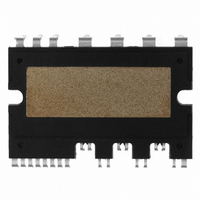
... Home appliances applications like air conditioner and wash- ing machine Top View 44mm 26.8mm ©2008 Fairchild Semiconductor Corporation FSBB15CH60C Rev. D Motion-SPM General Description advanced motion-smart power module (Motion-SPM that Fairchild has newly developed and designed to provide very compact and high performance ac motor drives mainly tar- geting low-power inverter-driven application like air conditioner and washing machine ...
Page 2
... For inverter low-side IGBTs: Gate drive circuit, Short circuit protection (SC) Control supply circuit under-voltage (UV) protection • Fault signaling: Corresponding to UV (Low-side supply) and SC faults • Input interface: 3.3/5V CMOS/LSTTL compatible, Schmitt trigger input Pin Configuration FSBB15CH60C Rev. D Top View Figure 2. 2 www.fairchildsemi.com ...
Page 3
... FSBB15CH60C Rev. D Pin Description Low-side Common Bias Voltage for IC and IGBTs Driving Common Supply Ground Signal Input for Low-side U Phase Signal Input for Low-side V Phase Signal Input for Low-side W Phase Fault Output Capacitor for Fault Output Duration Time Selection Capacitor (Low-pass Filter) for Short-Current Detection Input ...
Page 4
... Inverter low-side is composed of three IGBTs, freewheeling diodes for each IGBT and one control IC. It has gate drive and protection functions. 2. Inverter power side is composed of four inverter dc-link input terminals and three inverter output terminals. 3. Inverter high-side is composed of three IGBTs, freewheeling diodes and three drive ICs for each IGBT. FSBB15CH60C Rev. D (19) V B(W) ...
Page 5
... V Isolation Voltage ISO Thermal Resistance Symbol Parameter R Junction to Case Thermal th(j-c)Q Resistance R th(j-c)F Note: 2. For the measurement point of case temperature(T FSBB15CH60C Rev 25°C, Unless Otherwise Specified) J Conditions Applied between P- N Applied between 25° 25°C, Under 1ms Pulse Width 25°C per One Chip ...
Page 6
... BSD UV BSR t Fault-out Pulse Width FOD V ON Threshold Voltage IN(ON) V OFF Threshold Voltage IN(OFF) Note: 4. Short-circuit current protection is functioning only at the low-sides. 5. The fault-out pulse width t depends on the capacitance value of C FOD FSBB15CH60C Rev 25°C, Unless Otherwise Specified) J Conditions 15V I = 15A ...
Page 7
... SWITCHING LOSS(ON) VS. COLLECTOR CURRENT 800 V =300V CE V =15V 700 CC V =5V IN =25 ℃ T 600 J =150 ℃ 500 400 300 200 100 COLLECTOR CURRENT, I FSBB15CH60C Rev. D 100% I 100 C(ON) V 90% I 10% V IN(OFF Figure 4. Switching Time Definition 500 V 450 V V 400 350 300 250 ...
Page 8
... Supply Voltage PN V Control Supply Voltage CC V High-side Bias Voltage BS dV /dt, Control supply variation Blanking Time for Preventing dead Arm-short f PWM Input Signal PWM V Voltage for Current Sensing SEN FSBB15CH60C Rev. D Conditions I = 0.1A 25° 0.1A 25° Built in Bootstrap Diode V -I Characteristic ...
Page 9
... Mechanical Characteristics and Ratings Parameter Mounting Torque Mounting Screw Device Flatness Weight Package Marking and Ordering Information Device Marking Device FSBB15CH60C FSBB15CH60C FSBB15CH60C Rev. D Conditions Recommended 0.62N•m Note Figure Figure 7. Flatness Measurement Position Package Reel Size SPM27- Limits Units Min. ...
Page 10
... Normal operation: IGBT ON and carrying current Under voltage detection (UV BSD b4 : IGBT OFF in spite of control input condition, but there is no fault output signal Under voltage reset (UV ) BSR b6 : Normal operation: IGBT ON and carrying current Figure 9. Under-Voltage Protection (High-side) FSBB15CH60C Rev. D RESET SET UV CCR a1 UV CCD a3 ...
Page 11
... Fault output timer operation starts: The pulse width of the fault output signal is set by the external capacitor Input “L” : IGBT OFF state Input “H”: IGBT ON state, but during the active period of fault output the IGBT doesn’t turn ON IGBT OFF state Figure 10. Short-Circuit Current Protection (Low-side Operation only) FSBB15CH60C Rev SET RESET ...
Page 12
... These Values depend on PWM Control Algorithm 15V-Line 22uF 1000uF Note: 1) The ceramic capacitor placed between V -COM should be over 1uF and mounted as close to the pins of the SPM as possible. CC Figure 12. Recommended Bootstrap Operation Circuit and Parameters FSBB15CH60C Rev. D 5V-Line R =4.7㏀ PF 100Ω 100Ω 100Ω 1nF ...
Page 13
... Relays are used at almost every systems of electrical equipments of home appliances. In these cases, there should be sufficient distance between the CPU and the relays. should be over 1 μ F and mounted as close to the pins of the SPM as possible. 12) C SPC15 FSBB15CH60C Rev. D 15V line (19) V B(W ) ...
Page 14
... Detailed Package Outline Drawings FSBB15CH60C Rev www.fairchildsemi.com ...
Page 15
... Detailed Package Outline Drawings FSBB15CH60C Rev. D (Continued) 15 www.fairchildsemi.com ...
Page 16
... Detailed Package Outline Drawings FSBB15CH60C Rev. D (Continued) 16 www.fairchildsemi.com ...
Page 17
... TRADEMARKS The following are registered and unregistered trademarks and service marks Fairchild Semiconductor owns or is authorized to use and is not intended exhaustive list of all such trademarks. ® ACEx Build it Now™ CorePLUS™ CROSSVOLT ™ CTL™ Current Transfer Logic™ ® ...