GP1A91LC Sharp Microelectronics, GP1A91LC Datasheet

PHOTOINTER OPIC SLOT 1.2MM PCB

GP1A91LC

Manufacturer Part Number
GP1A91LC
Description
PHOTOINTER OPIC SLOT 1.2MM PCB
Manufacturer
Sharp Microelectronics
Series
OPIC™r
Datasheet

Specifications of GP1A91LC

Sensing Distance
0.047" (1.2mm)
Sensing Method
Transmissive
Output Configuration
NPN - Open Collector
Mounting Type
Through Hole
Current - Supply
700µA
Voltage - Supply
1.4 V ~ 7 V
Response Time
0.6µs, 0.2µs
Package / Case
PCB Mount
Lead Free Status / RoHS Status
Contains lead / RoHS non-compliant
Other names
425-1084-5

Available stocks

Company
Part Number
Manufacturer
Quantity
Price
Part Number:
GP1A91LC
Manufacturer:
SHARP
Quantity:
10 000
*1 The derating factors of absolute maximum ratings due to ambient temperature are
*2 For 5s or less
GP1A91LR/GP1A91LC
1. Compact package (3.7 2.6 3.1mm)
2. Can be directly connected to C-MOS logic and
3. Low voltage operation, low dissipation current
4. Gap width 1.2mm, slit width 0.23mm
5. General purpose
1. Cameras
2. CD-ROM drives
Input
Output
Notice
Internet Internet address for Electronic Components Group http://www.sharp.co.jp/ecg/
shown in Fig.3, 4, 5
microcomputer
(Operating supply voltage : 1.4 to 7.0V
OFF-state consumption current : MAX. 0.5mA)
Absolute Maximum Ratings
Features
Applications
*1
Reverse voltage
Power dissipation
Soldering temperature
In the absence of confirmation by device specification sheets, SHARP takes no responsibility for any defects that may occur in equipment using any SHARP
devices shown in catalogs, data books, etc. Contact SHARP in order to obtain the latest device specification sheets before using any SHARP device.
Forward current
Power dissipation
Supply voltage
Low level Output current
Operating temperature
Storage temperature
Parameter
Symbol
V
T
T
T
V
P
I
I
P
opr
CC
O
sol
stg
F
O
R
40 to 100
25 to 85
Rating
260
7.0
2.0
75
50
80
6
(Ta 25 C)
Unit
mW
mW
mA
mA
V
V
C
C
C
*“OPIC” (Optical IC) is a trademark of the SHARP Corporation. An OPIC consists
Subminiature OPIC
Photointerrupter
of a light-detecting element and signal-processing circuit integrated onto a single chip.
Outline Dimensions
1.25
0.3
4
3
2
Top view
1.2
2.65
3.7
0.15
(C0.3)
5
1
Emitter
Center
0.2
0.1
(C0.4)
Internal connection diagram : Top view
GP1A91LR
GP1A91LC
2
3
4
2
3
4
Unspecified tolerance : 0.2mm
( ) : Reference dimensions
The dimensions indicated by
those measured from the lead base.
(15k )
1.0
GP1A91LR/GP1A91LC
2.6
Soldering area
1mm
Amp.
Amp.
0.4
1.0
Residual
gates (2)
MIN.
0.6
1
1
5
5
1
2
3
4
5
(0.8)
(0.23)
(Unit : mm)
a-a' section
b-b' section
: Anode
: V
: V
: GND
: Cathode
CC
O
refer to

Related parts for GP1A91LC

GP1A91LC Summary of contents

Page 1

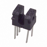
... GP1A91LR/GP1A91LC (Unit : mm) Internal connection diagram : Top view GP1A91LR (15k ) : Anode GND Cathode 5 Amp. GP1A91LC Amp. a-a' section (0.8) (C0.4) 2.6 Emitter Center 0.6 (C0.3) Residual gates (2) b-b' section 0.2 0.15 (0.23) 0.4 0.1 1.0 1 ...

Page 2

... I 1mA, I 5mA 3V, I 0mA 3V, I 5mA 3V, I 0mA FHL 5mA (GP1A91LR 2.4k (GP1A91LC (Condition during measureing response time : (15k ) 0.1 F GND 2. 0.1 F GND MIN. TYP. MAX. 1.15 1.25 10 1.4 7.0 0.1 0.4 2.9 0.7 1.2 0.3 0.5 3.5 1.2 0.8 ...

Page 3

... Fig.8 Relative Threshold Input Current vs. GP1A91LR FHL 7.5 10 (V) CC Temperature 2.5 2 1 Ambient temperature 500 200 25 C 100 0.5 1 1.5 2 2.5 Forward voltage V (V) F Supply Voltage GP1A91LC 1.2 I FHL 1.0 0.8 I FLH 0.6 0.4 0 2.5 5 7.5 Supply voltage V (V) CC 100 3 3 FHL ...

Page 4

... Current vs. Supply Voltage (1) GP1A91LC I :I CCL 2 CCH T 1 15k L 1.6 1.4 1.2 I CCL 1.0 0.8 0.6 0.4 I CCH 0 Supply voltage V (V) CC Current vs. Supply Voltage (2) GP1A91LC I CCL 2.0 I CCH 1 15k L 1.6 1.4 1.2 I CCL 1.0 0.8 0.6 0.4 I CCH 0 Supply voltage V (V) CC 100 5mA F ...

Page 5

... CC Level Output Current GP1A91LC I 5mA F 200 180 160 140 120 100 0.3 0.6 0.9 1.2 1.5 1.8 2.1 2.4 2.7 Low level output current I (mA) OL Ambient Temperature GP1A91LC 0.4 I 5mA 0.3 0.2 I 2mA OL 0.1 I 1mA OL I 0mA Ambient temperature 5mA ...

Page 6

... Fig.24 Propagation Delay Time vs. Forward GP1A91LR t PLH t PHL 40 50 (mA) F Fig.26 Low, High Level Output vs. Shield Distance 2 3 Resistance GP1A91LC 1 5mA 1 1.2 1.0 0.8 0.6 0.4 0 Load resistance Current GP1A91LC 2. PLH PHL Forward current I (mA) F (2) (Typical Value) I 5mA Shield High L 0 Sensor Low 1 ...

Page 7

Application Circuits NOTICE The circuit application examples in this publication are provided to explain representative applications of SHARP devices and are not intended to guarantee any circuit design or license any intellectual property rights. SHARP takes no responsibility for any ...

Related keywords