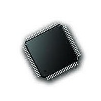
PIC18F86J72-I/PT Microchip Technology, PIC18F86J72-I/PT Datasheet - Page 177

PIC18F86J72-I/PT
Manufacturer Part Number
PIC18F86J72-I/PT
Description
IC PIC MCU 8BIT 14KB FLSH 80TQFP
Manufacturer
Microchip Technology
Series
PIC® 18Fr
Datasheet
1.PIC18F86J72-IPT.pdf
(480 pages)
Specifications of PIC18F86J72-I/PT
Program Memory Type
FLASH
Program Memory Size
64KB (32K x 16)
Package / Case
80-TQFP
Core Processor
PIC
Core Size
8-Bit
Speed
48MHz
Connectivity
I²C, LIN, SPI, UART/USART
Peripherals
Brown-out Detect/Reset, LCD, LVD, POR, PWM, WDT
Number Of I /o
51
Ram Size
3.8K x 8
Voltage - Supply (vcc/vdd)
2 V ~ 3.6 V
Data Converters
A/D 12x12b
Oscillator Type
Internal
Operating Temperature
-40°C ~ 85°C
Data Bus Width
8 bit
Data Ram Size
4 KB
Interface Type
SPI, USART, SPI, I2C
Maximum Clock Frequency
8 MHz
Number Of Programmable I/os
51
Number Of Timers
4
Operating Supply Voltage
2 V to 3.6 V
Maximum Operating Temperature
+ 85 C
Mounting Style
SMD/SMT
Minimum Operating Temperature
- 40 C
On-chip Adc
14
Controller Family/series
PIC18F
No. Of I/o's
51
Ram Memory Size
3923Byte
Cpu Speed
12MIPS
No. Of Timers
4
Rohs Compliant
Yes
Lead Free Status / RoHS Status
Lead free / RoHS Compliant
Lead Free Status / RoHS Status
Lead free / RoHS Compliant, Lead free / RoHS Compliant
Available stocks
Company
Part Number
Manufacturer
Quantity
Price
Company:
Part Number:
PIC18F86J72-I/PT
Manufacturer:
Microchip Technology
Quantity:
10 000
- Current page: 177 of 480
- Download datasheet (5Mb)
17.3.4
When designing applications that use the LCD regula-
tor with the charge pump enabled, users must always
consider both the dynamic current and RMS (static)
current requirements of the display, and what the
charge pump can deliver. Both dynamic and static
current can be determined by Equation 17-1:
EQUATION 17-1:
For dynamic current, C is the value of the capacitors
attached to LCDBIAS3 and LCDBIAS2. The variable,
dV, is the voltage drop allowed on C2 and C3 during a
voltage switch on the LCD display, and dT is the dura-
tion of the transient current after a clock pulse occurs.
For practical design purposes, these will be assumed
to be 0.047 F for C, 0.1V for dV and 1 s for dT. This
yields a dynamic current of 4.7 mA for 1 s.
RMS current is determined by the value of C
the voltage across V
regulator clock period (T
0.047 F, a value of 1.02V across C
30 s, the maximum theoretical static current will be
1.8 mA. Since the charge pump must charge five
capacitors, the maximum current becomes 360 A. For
a real-world assumption of 50% efficiency, this yields a
practical current of 180 A.
Users should compare the calculated current capacity
against the requirements of the LCD. While dV and dT
are relatively fixed by device design, the values of C
and the capacitors on the LCDBIAS pins can be
changed to increase or decrease current. As always,
any changes should be evaluated in the actual circuit
for its impact on the application.
2010 Microchip Technology Inc.
DESIGN CONSIDERATIONS FOR
THE LCD CHARGE PUMP
LCAP
I = C x
PER
1 and V
) for dT. Assuming C
dV
dT
LCAP
FLY
2 for dV and the
and T
FLY
PER
FLY
for C,
Preliminary
FLY
of
of
PIC18F87J72 FAMILY
17.4
The LCD driver module can be configured into four
multiplex types:
• Static (only COM0 used)
• 1/2 Multiplex (COM0 and COM1 are used)
• 1/3 Multiplex (COM0, COM1 and COM2 are used)
• 1/4 Multiplex (all COM0, COM1, COM2 and COM3
The number of active commons used is configured by
the LMUX<1:0> bits (LCDCON<1:0>), which deter-
mines the function of the PORTE<6:4> pins (see
Table 17-3 for details). If the pin is configured as a COM
drive, the port I/O function is disabled and the TRIS
setting of that pin is overridden.
TABLE 17-3:
17.5
The LCDSEx registers are used to select the pin
function for each segment pin. Setting a bit configures
the corresponding pin to function as a segment driver.
LCDSEx registers do not override the TRIS bit settings,
so the TRIS bits must be configured as input for that
pin.
17.6
The LCDDATAx registers contain bits which define the
state of each pixel. Each bit defines one unique pixel.
Table 17-2 shows the correlation of each bit in the
LCDDATAx registers to the respective common and
segment signals. Any LCD pixel location not being
used for display can be used as general purpose RAM.
LMUX<1:0> PORTE<6>
are used)
Note:
Note:
00
01
10
11
LCD Multiplex Types
Segment Enables
Pixel Control
On a Power-on Reset, the LMUX<1:0>
bits are ‘00’.
On a Power-on Reset, these pins are
configured as digital I/O.
COM3 Driver COM2 Driver COM1 Driver
Digital I/O
Digital I/O
Digital I/O
PORTE<6:4> FUNCTION
COM2 Driver COM1 Driver
PORTE<5>
Digital I/O
Digital I/O
DS39979A-page 177
COM1 Driver
PORTE<4>
Digital I/O
Related parts for PIC18F86J72-I/PT
Image
Part Number
Description
Manufacturer
Datasheet
Request
R

Part Number:
Description:
Manufacturer:
Microchip Technology Inc.
Datasheet:

Part Number:
Description:
Manufacturer:
Microchip Technology Inc.
Datasheet:

Part Number:
Description:
Manufacturer:
Microchip Technology Inc.
Datasheet:

Part Number:
Description:
Manufacturer:
Microchip Technology Inc.
Datasheet:

Part Number:
Description:
Manufacturer:
Microchip Technology Inc.
Datasheet:

Part Number:
Description:
Manufacturer:
Microchip Technology Inc.
Datasheet:

Part Number:
Description:
Manufacturer:
Microchip Technology Inc.
Datasheet:

Part Number:
Description:
Manufacturer:
Microchip Technology Inc.
Datasheet:


