TBU-KE050-500-WH Bourns Inc., TBU-KE050-500-WH Datasheet

SURGE SUPP TBU 500MA 500VIMP SMD

TBU-KE050-500-WH

Manufacturer Part Number
TBU-KE050-500-WH
Description
SURGE SUPP TBU 500MA 500VIMP SMD
Manufacturer
Bourns Inc.
Series
TBU™r

Specifications of TBU-KE050-500-WH

Package / Case
2-VDFN Exposed Pad
Voltage - Working
250V
Voltage - Clamping
500V
Technology
Mixed Technology
Number Of Circuits
1
Applications
General Purpose
Voltage Rating
250 V
Current Rating
750 mA
Termination Style
SMD/SMT
Operating Voltage
500V
Diode Case Style
DFN
No. Of Pins
2
Rohs Compliant
Yes
Lead Free Status / RoHS Status
Lead free / RoHS Compliant
Power (watts)
-
Lead Free Status / Rohs Status
Lead free / RoHS Compliant
Other names
TBU-KE050-500-WHTR
The TBU-KE Series of Bourns
(Transient Blocking Unit) products are very
low capacitance unidirectional high speed
surge protection components designed to protect
against faults caused by short circuits, AC
power cross, induction and lightning surges.
The TBU-KE is a unidirectional TBU
1 μs when the current reaches the maximum value in one direction only, that is when
Pin 1 is positive in voltage with respect to Pin 2. No current limiting exists in the oppo-
site polarity, and the TBU
should not exceed the maximum trip current level of the TBU
diode may be used to prevent reverse current in DC biased applications.
The TBU
sitive electronics will not be exposed to large voltages or currents during surge events.
After the surge, the TBU
to the V
bias or have DC bias below V
The TBU
standard requirements such as RoHS and Pb Free solder refl ow profi les.
*RoHS Directive 2002/95/EC Jan 27, 2003 including Annex.
Specifi cations are subject to change without notice.
Customers should verify actual device performance in their specifi c applications.
Symbol
V
V
T
T
General Information
Absolute Maximum Ratings (@ T
op
stg
imp
rms
reset
®
®
protector blocks surges and provides an effective barrier behind which sen-
device is provided in a surface mount DFN package and meets industry
level. The TBU
Parameter
Peak impulse voltage withstand with duration less than 10 ms
Continuous A.C. RMS voltage
Operating temperature range
Storage temperature range
®
®
device resets when the voltage across the TBU
protector appears as resistive in nature. The reverse current
®
device will automatically reset on lines which have no DC
reset
®
TBU
(such as unpowered signal lines).
Asia-Pacifi c: Tel: +886-2 2562-4117 • Fax: +886-2 2562-4116
Europe: Tel: +41-41 768 5555 • Fax: +41-41 768 5510
The Americas: Tel: +1-951 781-5500 • Fax: +1-951 781-5700
www.bourns.com
®
®
A
device: the TBU
= 25 °C Unless Otherwise Noted)
TBU-KE Series - TBU
Features
Superior circuit protection
Overcurrent and overvoltage protection
Blocks surges up to rated limits
High speed performance
Small SMT package
RoHS compliant*
Agency recognition:
Line Side
®
protector will trip in less than
®
TBU
1
device. An external
®
Device
2
®
device falls
TBU-KE025-xxx-WH
TBU-KE040-xxx-WH
TBU-KE050-xxx-WH
TBU-KE025-xxx-WH
TBU-KE040-xxx-WH
TBU-KE050-xxx-WH
Load Side
®
Part Number
High Speed Protectors
Applications
UL
Set top box LNB ports
Protection modules and dongles
Process control equipment
Test and measurement equipment
General electronics
Agency Approval
-65 to +150
-40 to +85
File Number: E315805
Value
250
400
500
100
200
250
Description
Unit
°C
°C
V
V

Related parts for TBU-KE050-500-WH

TBU-KE050-500-WH Summary of contents

Page 1

... Pin 1 is positive in voltage with respect to Pin 2. No current limiting exists in the oppo- site polarity, and the TBU ® protector appears as resistive in nature. The reverse current should not exceed the maximum trip current level of the TBU diode may be used to prevent reverse current in DC biased applications. ® The TBU protector blocks surges and provides an effective barrier behind which sen- sitive electronics will not be exposed to large voltages or currents during surge events ...

Page 2

... V I (min.) = 200 mA TBU-KE050-200-WH trigger = 500 V I (min.) = 300 mA TBU-KE050-300-WH trigger = 500 V I (min.) = 500 mA TBU-KE050-500-WH trigger ® device with 50 Vdc circuit voltage ® device will transition to normal operating 2 ) Customers should verify actual device performance in their specifi c applications. Min. ...

Page 3

... Customers should verify actual device performance in their specifi c applications. ® High Speed Protectors Basic TBU Operation The TBU device which is placed in series with a signal path. The TBU device operates in approximately 1 µs - once line current exceeds the TBU ated, the TBU typically. When operated, the TBU voltages and any other voltages including the surge up to rated limits ...

Page 4

... TBU-KE Series - TBU Performance Graphs (Continued) Power Derating Curve 3.0 No additional PCB Cu 2.5 0.5 sq. in. additional PCB CU 2.0 1.5 1.0 0.5 0 Junction Temperature (°C) Refl ow Profi le Profi le Feature Average Ramp-Up Rate (Tsmax to Tp) Preheat - Temperature Min. (Tsmin) - Temperature Max. (Tsmax) ...

Page 5

... TBU-KE Series - TBU Product Dimensions 5.00 ± 0.10 (.197 ± .004) 2.50 ± 0.10 (.098 ± .004) PIN 1 & BACKSIDE CHAMFER 1.00 (.039) Recommended Pad Layout ® TBU protectors have matte-tin termination fi nish. The suggested layout should use Non-Solder Mask Defi ne (NSMD). ...

Page 6

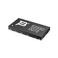
... Bourns, Inc. in the U.S., Taiwan and European Community. Specifi cations are subject to change without notice. Customers should verify actual device performance in their specifi c applications. ® High Speed Protectors Typical Part Marking ...

Related keywords