TBU-PL060-200-WH Bourns Inc., TBU-PL060-200-WH Datasheet
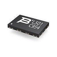
SURGE SUPP TBU DL 50OHM 600VIMP

TBU-PL060-200-WH

Manufacturer Part Number
TBU-PL060-200-WH
Description
SURGE SUPP TBU DL 50OHM 600VIMP
Manufacturer
Bourns Inc.
Series
TBU™r

Specifications of TBU-PL060-200-WH

Package / Case
SMD 6.50mm x 4.00mm
Voltage - Working
350V
Voltage - Clamping
600V
Technology
Mixed Technology
Number Of Circuits
2
Applications
SLIC
Voltage Rating
600 V
Current Rating
200 mA
Height
0.85 mm
Length
6.5 mm
Termination Style
SMD/SMT
Width
4 mm
Diode Type
Low Capacitance
Operating Voltage
-20V
Diode Case Style
DFN
No. Of Pins
8
Peak Surge Current
500A
Output Current
700µA
Suppressor Type
Transient Voltage
Rohs Compliant
Yes
Lead Free Status / RoHS Status
Lead free / RoHS Compliant
Power (watts)
-
Lead Free Status / Rohs Status
Lead free / RoHS Compliant
Other names
TBU-PL060-200-WHTR
The TBU-PL Series of Bourns
protection components, constructed using MOSFET semiconductor technology, and designed to
protect against faults caused by short circuits, AC power cross, induction and lightning surges.
In addition to overcurrent protection, an added feature is the voltage monitoring on the two lines. If the
voltage on the line drops below V ss then the voltage will trigger the device to switch to the blocking
state.
The TBU
detection circuit triggering to provide an effective barrier behind which sensitive electronics will not be
exposed to large voltages or currents during surge events. The TBU
mount DFN package and meets industry standard requirements such as RoHS and Pb Free solder
refl ow profi les.
*RoHS Directive 2002/95/EC Jan 27, 2003 including Annex.
Specifi cations are subject to change without notice.
Customers should verify actual device performance in their specifi c applications.
UL
Symbol
V
V
T
T
T
ESD
Symbol
I
R
R
t
I
I
V
V
V
R
R
R
R
trigger
Q
ss
block
General Information
Absolute Maximum Ratings (@ T
Electrical Characteristics (@ T
Agency Approval
op
stg
jmax
imp
rms
reset
to
ss
device
match
th(j-l)
th(j-l)
th(j-l)
th(j-l)
®
high-speed protector placed in the system circuit will monitor the current with the MOSFET
File Number: E315805
Parameter
Peak impulse voltage withstand with duration less than 10 ms
Continuous A.C. RMS voltage
Operating temperature range
Storage temperature range
Maximum Junction Temperature
HBM ESD Protection per IEC 61000-4-2 on line pads
Parameter
Current required for the device to go from operating state to
protected state
Series resistance of the TBU
Package resistance matching of the TBU
Time taken for the device to go into current limiting
Current through the triggered TBU
Operating current with V
Voltage below which the triggered TBU
transition to normal operating state
Voltage threshold offset with 60 Hz applied voltage, with V
Operating voltage range relative to V
One side junction to package pads - FR4 using minimum recommended pad layout
Both sides junction to package pads - FR4 using minimum recommended pad layout
One side junction to package pads - FR4 using heat sink on board (6 cm
Both sides junction to package pads - FR4 using heat sink on board (6 cm
Description
®
TBU
®
A
products are low capacitance dual bidirectional high-speed
= 25 °C Unless Otherwise Noted)
A
ss
= 25 °C Unless Otherwise Noted)
= -50 V
®
device
TBU-PL Series - TBU
®
Features
Solutions available for GR-1089-CORE, ITU-T and a combination of both.
device with 50 Vdc circuit voltage
dd
Industry Standards (in Conjunction with OVP Device)
Superior circuit protection
Overcurrent & overvoltage protection
Blocks surges up to rated limits
High-speed performance
Small SMT package
RoHS compliant*
Agency recognition:
®
device will
®
device #1 - TBU
®
device is provided in a surface
ss
®
device #2
-50 V (V
Part Number
TBU-PLxxx-100-WH
TBU-PLxxx-200-WH
TBU-PLxxx-100-WH
TBU-PLxxx-200-WH
TBU-PL050-xxx-WH
TBU-PL060-xxx-WH
TBU-PL075-xxx-WH
TBU-PL085-xxx-WH
TBU-PL050-xxx-WH
TBU-PL060-xxx-WH
TBU-PL075-xxx-WH
TBU-PL085-xxx-WH
®
ss
Part Number
- V
High-Speed Protectors
2
) (0.5 in.
2
lineSLIC
) (0.5 in.
2
)
Applications
)
2
)
SLIC protection
Cable & DSL
MDU/MTU modems
ONT
Voice/DSL line cards
Min.
-180
0.25
100
200
-1.0
40
12
15
-55 to +125
-65 to +150
Line 1 SLIC
Line 2 SLIC
Value
+125
500
600
750
850
300
350
400
425
±2
Typ.
±0.5
0.70
150
300
100
110
50
15
20
65
40
70
TBU
Max.
®
±1.0
1.50
200
400
0.2
-20
55
22
25
Device
V dd
V ss
1
Unit
°C
°C
°C
kV
V
V
Line 1
Line 2
°C/W
°C/W
°C/W
°C/W
Unit
mA
mA
µA
µs
Ω
Ω
V
V
V

Related parts for TBU-PL060-200-WH

TBU-PL060-200-WH Summary of contents

Page 1

... MOSFET detection circuit triggering to provide an effective barrier behind which sensitive electronics will not be exposed to large voltages or currents during surge events. The TBU mount DFN package and meets industry standard requirements such as RoHS and Pb Free solder refl ...

Page 2

... Bourns protection devices with a pair of Bourns sensitive applications, a Bourns ® GDT may be substituted for the MOV. If EN55024 EMC compliance is required, the TBU device may require capacitors to be fi tted between the Tip and Ring connections and ground. GND 2 ...

Page 3

... GDT Special Test Protector with DC breakdown (DCBD) of less than 330 V. Notes: 1) The Le9500, Le9520 and Le9530 (VE950 series) require a 200 mA I trigger TBU the 100 mA device. 2) The MOV maximum continuous rms voltage rating should not be exceeded. The exception is where the data sheet highlights withstand ...

Page 4

... TBU-PL Series - TBU Performance Graphs Typical V-I Characteristics (TBU-PL085-200-WH) I CURRENT TRIGGER (50 mA/div) Tracking Voltage Characteristics V bat range of - -150 V 100 Voltage threshold offset (V) Power Derating Curve 3.0 One Side, No PCB Cu One Side, 0.5 sq. in. PCB Cu 2.5 Two Sides, No PCB Cu Two Sides, 0.5 sq. in. PCB Cu 2 ...

Page 5

... PCB copper areas which extend beyond the exposed solder pad. The exposed solder pads should be defi ned by a solder mask which matches the pad layout of the TBU size and spacing recommended that they should be the same dimension as the TBU ® ...

Page 6

... Time (tsmin to tsmax) Time maintained above: - Temperature (TL) - Time (tL) Peak/Classifi cation Temperature (Tp) Time within 5 °C of Actual Peak Temp. (tp) Ramp-Down Rate Time 25 °C to Peak Temperature How to Order TBU - PL 085 - 100 - WH ® TBU Product Series PL = Dual Bidirectional Series Impulse Voltage Rating 050 = 500 V 060 = 600 V ...

Page 7

... REV. 07/11 “TBU” registered trademark of Bourns, Inc. in the U.S., Taiwan and European Community. Specifi cations are subject to change without notice. Customers should verify actual device performance in their specifi c applications. High-Speed Protectors D t TOP ...

Related keywords