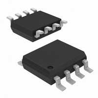
DMS3019SSD-13 Diodes Inc, DMS3019SSD-13 Datasheet - Page 2

DMS3019SSD-13
Manufacturer Part Number
DMS3019SSD-13
Description
MOSFET 2N-CH 30V 7A/5.7A SO8
Manufacturer
Diodes Inc
Datasheet
1.DMS3019SSD-13.pdf
(10 pages)
Specifications of DMS3019SSD-13
Fet Type
2 N-Channel (Dual)
Fet Feature
Logic Level Gate
Rds On (max) @ Id, Vgs
15 mOhm @ 9A, 10V
Drain To Source Voltage (vdss)
30V
Current - Continuous Drain (id) @ 25° C
7A, 5.7A
Vgs(th) (max) @ Id
2.4V @ 250µA
Gate Charge (qg) @ Vgs
42nC @ 10V
Input Capacitance (ciss) @ Vds
1932pF @ 15V
Power - Max
1.19W
Mounting Type
Surface Mount
Package / Case
8-SOIC (0.154", 3.90mm Width)
Configuration
Dual
Transistor Polarity
N-Channel
Resistance Drain-source Rds (on)
10 mOhms
Gate Charge Qg
42 nC
Forward Transconductance Gfs (max / Min)
5 S
Drain-source Breakdown Voltage
30 V
Gate-source Breakdown Voltage
20 V
Continuous Drain Current
7 A
Power Dissipation
1.19 W
Maximum Operating Temperature
+ 150 C
Mounting Style
SMD/SMT
Minimum Operating Temperature
- 55 C
Lead Free Status / RoHS Status
Lead free / RoHS Compliant
Other names
DMS3019SSD-13DITR
Maximum Ratings – Q1
Maximum Ratings – Q2
Thermal Characteristics
Drain-Source Voltage
Gate-Source Voltage
Continuous Drain Current (Note 4) V
Continuous Drain Current (Note 5) V
Continuous Drain Current (Note 5) V
Pulsed Drain Current (Note 6)
Avalanche Current (Notes 6 & 7)
Repetitive Avalanche Energy (Notes 6 & 7) L = 0.3mH
Drain-Source Voltage
Gate-Source Voltage
Continuous Drain Current (Note 4) V
Continuous Drain Current (Note 5) V
Continuous Drain Current (Note 5) V
Pulsed Drain Current (Note 6)
Avalanche Current (Notes 6 & 7)
Repetitive Avalanche Energy (Notes 6 & 7) L = 0.1mH
Power Dissipation (Note 4)
Thermal Resistance, Junction to Ambient @T
Power Dissipation (Note 5)
Thermal Resistance, Junction to Ambient @T
Operating and Storage Temperature Range
Notes:
DMS3019SSD
Document number: DS35053 Rev. 2 - 2
4. Device mounted on FR-4 substrate PC board, with minimum recommended pad layout. The value in any given application depends on the user’s specific
5. Device mounted on 1 inch x 1 inch FR4 PCB with high coverage of single sided 1oz copper, in still air conditions. Device contains two active die running
6. Repetitive rating, pulse width limited by junction temperature.
7. I
board design. Device contains two active die running at equal power.
at equal power.
AR
and E
AR
rating are based on low frequency and duty cycles to keep T
GS
GS
GS
GS
GS
GS
@TA = 25°C unless otherwise specified
@TA = 25°C unless otherwise specified
Characteristic
Characteristic
Characteristic
= 10V
= 10V
= 4.5V
= 10V
= 10V
= 4.5V
A
A
= 25°C (Note 4)
= 25°C (Note 5)
Steady
Steady
Steady
Steady
Steady
Steady
State
State
State
State
State
State
www.diodes.com
T
T
T
T
T
T
T
T
T
T
T
T
2 of 10
A
A
A
A
A
A
A
A
A
A
A
A
J
= 25°C
= 25°C
= 70°C
= 25°C
= 70°C
= 25°C
= 70°C
= 25°C
= 70°C
= 25°C
= 70°C
= 25°C
= 70°C
Symbol
Symbol
Symbol
T
V
V
J
V
V
R
R
E
E
I
,
I
I
P
P
DSS
GSS
I
I
I
DM
DSS
GSS
I
I
I
I
AR
AR
T
θJA
θJA
AR
AR
D
D
D
D
D
D
D
D
D
STG
-55 to +150
Value
Value
Value
25.4
12.8
1.19
1.79
±12
±20
107
7.0
5.6
9.0
7.0
8.0
6.5
5.7
4.6
7.0
5.6
6.0
4.7
30
40
13
30
40
16
70
DMS3019SSD
© Diodes Incorporated
October 2010
°C/W
°C/W
Unit
Unit
Unit
mJ
mJ
°C
W
W
V
V
A
A
A
A
A
V
V
A
A
A
A
A


