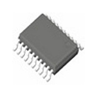
ICS83056AGI-01LF IDT, Integrated Device Technology Inc, ICS83056AGI-01LF Datasheet - Page 2

ICS83056AGI-01LF
Manufacturer Part Number
ICS83056AGI-01LF
Description
IC CLK MUX 2:6 250MHZ 20TSSOP
Manufacturer
IDT, Integrated Device Technology Inc
Type
Multiplexerr
Series
HiPerClockS™r
Datasheet
1.ICS83056AGI-01LF.pdf
(14 pages)
Specifications of ICS83056AGI-01LF
Number Of Circuits
1
Ratio - Input:output
2:6
Differential - Input:output
No/No
Input
LVCMOS, LVTTL
Output
LVCMOS, LVTTL
Frequency - Max
250MHz
Voltage - Supply
2.375 V ~ 3.465 V
Operating Temperature
-40°C ~ 85°C
Mounting Type
Surface Mount
Package / Case
20-TSSOP (0.173", 4.40mm Width)
Frequency-max
250MHz
Number Of Clock Inputs
2
Mode Of Operation
Single-Ended
Output Frequency
250MHz
Output Logic Level
LVCMOS/LVTTL
Operating Supply Voltage (min)
2.375V
Operating Supply Voltage (typ)
2.5/3.3V
Operating Supply Voltage (max)
3.465V
Package Type
TSSOP
Operating Temp Range
-40C to 85C
Operating Temperature Classification
Industrial
Signal Type
LVCMOS/LVTTL
Mounting
Surface Mount
Pin Count
20
Lead Free Status / RoHS Status
Lead free / RoHS Compliant
Available stocks
Company
Part Number
Manufacturer
Quantity
Price
Company:
Part Number:
ICS83056AGI-01LF
Manufacturer:
IDT
Quantity:
485
Table 1. Pin Descriptions
NOTE: Pullup and Pulldown refer to internal input resistors. See Table 2, Pin Characteristics, for typical values.
Table 2. Pin Characteristics
Function Tables
Table 3. Control Input Function Table
IDT™ / ICS™ 2:1, SINGLE-ENDED LVCMOS MULTIPLEXER
Symbol
C
C
R
R
R
ICS83056I-01
6-BIT, 2:1, SINGLE-ENDED LVCMOS MULTIPLEXER
12, 16, 19
IN
PD
PULLUP
PULLDOWN
OUT
Number
Control Inputs
10, 11
15, 20
2, 5, 9
3, 18
4, 17
7, 14
1, 6
13
8
SELx
0
1
Parameter
Input Capacitance
Power Dissipation Capacitance
(per output)
Input Pullup Resistor
Input Pulldown Resistor
Output Impedance
SEL5, SEL4,
SEL3, SEL2,
CLK1, CLK0
SEL1, SEL0
Q5, Q4, Q3,
Q2, Q1, Q0
Name
V
GND
V
OE
DDO
DD
Outputs
CLK0
CLK1
Qx
Output
Power
Power
Power
Input
Input
Input
Type
Pulldown
Pulldown
Pullup
V
V
DD
DD
V
Test Conditions
V
V
DD
= V
= V
DDO
DDO
Description
Clock select inputs. See Table 3. LVCMOS / LVTTL interface levels.
Single-ended clock output. LVCMOS/LVTTL interface levels.
Output supply pins.
Power supply ground.
Single-ended clock inputs. LVCMOS/LVTTL interface levels.
Power supply pin.
Output enable. When LOW, outputs are in a High impedance state.
When HIGH, outputs are active. LVCMOS / LVTTL interface levels.
V
= V
DDO
DDO
DDO
= 3.465V
= 2.625V
DDO
= 2V
2
= 3.465V
= 2.625V
= 2V
Minimum
ICS83056AGI-01 REV. A JANUARY 29, 2009
Typical
18
19
19
51
51
15
17
25
4
Maximum
Units
k
k
pF
pF
pF
pF
Ω
Ω
Ω
Ω
Ω


