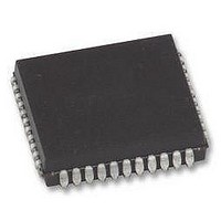
AT89LP52-20JU Atmel, AT89LP52-20JU Datasheet - Page 13

AT89LP52-20JU
Manufacturer Part Number
AT89LP52-20JU
Description
IC MCU 8051 8K FLASH SPI 44PLCC
Manufacturer
Atmel
Series
89LPr
Datasheet
1.AT89LP52-20MU.pdf
(113 pages)
Specifications of AT89LP52-20JU
Core Processor
8051
Core Size
8-Bit
Speed
20MHz
Connectivity
EBI/EMI, I²C, SPI, UART/USART
Peripherals
Brown-out Detect/Reset, POR, PWM, WDT
Number Of I /o
36
Program Memory Size
8KB (8K x 8)
Program Memory Type
FLASH
Ram Size
256 x 8
Voltage - Supply (vcc/vdd)
2.4 V ~ 5.5 V
Oscillator Type
Internal
Operating Temperature
-40°C ~ 85°C
Package / Case
44-LCC (J-Lead)
Processor Series
AT89x
Core
8051
Data Bus Width
8 bit
Data Ram Size
256 B
Interface Type
Serial
Maximum Clock Frequency
20 MHz
Number Of Programmable I/os
36
Number Of Timers
3
Operating Supply Voltage
2.7 V to 5.5 V
Maximum Operating Temperature
+ 85 C
Mounting Style
SMD/SMT
Lead Free Status / RoHS Status
Lead free / RoHS Compliant
Eeprom Size
-
Data Converters
-
Lead Free Status / Rohs Status
Details
Available stocks
Company
Part Number
Manufacturer
Quantity
Price
Company:
Part Number:
AT89LP52-20JU
Manufacturer:
Atmel
Quantity:
110
3.2.1
3.2.2
3.2.3
3.3
3.3.1
3709B–MICRO–12/10
External Data Memory
DATA
IDATA
SFR
XDATA
Figure 3-5.
The first 128 bytes of RAM are directly addressable by an 8-bit address (00H–7FH) included in
the instruction. The lowest 32 bytes of DATA memory are grouped into 4 banks of 8 registers
each. The RS0 and RS1 bits (PSW.3 and PSW.4) select which register bank is in use. Instruc-
tions using register addressing will only access the currently specified bank. The lower 128 bit
addresses are also mapped into DATA addresses 20H—2FH.
The full 256 byte internal RAM can be indirectly addressed using the 8-bit pointers R0 and R1.
The first 128 bytes of IDATA include the DATA space. The hardware stack is also located in the
IDATA space.
The upper 128 direct addresses (80H–FFH) access the I/O registers. I/O registers on AT89LP
devices are referred to as Special Function Registers. The SFRs can only be accessed through
direct addressing. All SFR locations are not implemented. See
SFRs.
AT89LP microcontrollers support a 16-bit external memory address space for up to 64K bytes of
external data memory (XDATA). The external memory space is accessed with the MOVX
instructions. Some internal data memory resources are mapped into portions of the external
address space as shown in
the CPU can access them. The AT89LP51/52 includes 256 bytes of nonvolatile Flash data
memory (FDATA).
The external data memory space can accommodate up to 64KB of external memory. The
AT89LP51/52 uses the standard 8051 external data memory interface with the upper address
byte on Port 2, the lower address byte and data in/out multiplexed on Port 0, and the ALE, RD
and WR strobes. XDATA can be accessed with both 16-bit (MOVX @DPTR) and 8-bit (MOVX
@Ri) addresses. See
interface.
LOWER
UPPER
128
128
Internal Data Memory Map
FFH
7FH
80H
0
AND INDIRECT
Section 3.3.3 on page 17
ADDRESSING
ADDRESSING
BY INDIRECT
ACCESSIBLE
ACCESSIBLE
DATA/IDATA
BY DIRECT
Figure
IDATA
ONLY
3-6. These memory spaces may require configuration before
AT89LP51/52 - Preliminary
ADDRESSING
ACCESSIBLE
BY DIRECT
SFR
SPECIAL
FUNCTION
REGISTERS
for more details of the external memory
FFH
80H
Section 4.
PORTS
STATUS AND
CONTROL BITS
TIMERS
REGISTERS
STACK POINTER
ACCUMULATOR
(ETC.)
for a listed of available
13


