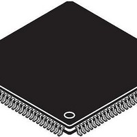
MCF51MM128VLK Freescale Semiconductor, MCF51MM128VLK Datasheet - Page 45

MCF51MM128VLK
Manufacturer Part Number
MCF51MM128VLK
Description
IC MCU 32BIT 128K COLDF 81-LQFP
Manufacturer
Freescale Semiconductor
Series
MCF51MMr
Datasheet
1.TWR-MCF51MM.pdf
(58 pages)
Specifications of MCF51MM128VLK
Core Processor
Coldfire V1
Core Size
32-Bit
Speed
50MHz
Connectivity
CAN, EBI/EMI, I²C, SCI, SPI, USB OTG
Peripherals
LVD, PWM, WDT
Number Of I /o
47
Program Memory Size
128KB (128K x 8)
Program Memory Type
FLASH
Ram Size
32K x 8
Voltage - Supply (vcc/vdd)
1.8 V ~ 3.6 V
Data Converters
A/D 8x16b, D/A 1x12b
Oscillator Type
External
Operating Temperature
-40°C ~ 105°C
Package / Case
80-LQFP
Core
ColdFire V1
Data Bus Width
32 bit
Data Ram Size
32 KB
Interface Type
SCI, SPI, I2C, USB
Maximum Clock Frequency
50.3 MHz
Operating Supply Voltage
1.8 V to 3.6 V
Maximum Operating Temperature
+ 105 C
Mounting Style
SMD/SMT
Minimum Operating Temperature
- 40 C
Package
80LQFP
Device Core
ColdFire
Family Name
MCF51MM
Maximum Speed
50.33 MHz
Number Of Programmable I/os
47
On-chip Adc
8-chx16-bit
On-chip Dac
1-chx12-bit
Number Of Timers
1
Lead Free Status / RoHS Status
Lead free / RoHS Compliant
Eeprom Size
-
Lead Free Status / Rohs Status
Details
Available stocks
Company
Part Number
Manufacturer
Quantity
Price
Company:
Part Number:
MCF51MM128VLK
Manufacturer:
Freescale Semiconductor
Quantity:
10 000
3.13
Table 23
Freescale Semiconductor
Freescale reserves the right to change the detail specifications as may be required to permit improvements in the design of its products.
1
2
3
4
No.
Numbers in this column identify elements in
All timing is shown with respect to 20% V
rate control disabled and high drive strength enabled for SPI output pins.
Time to data active from high-impedance state.
Hold time to high-impedance state.
10
11
12
13
1
2
3
4
5
6
7
8
9
and
SPI Characteristics
1
SPSCK period
Slave MISO disable time
Operating frequency
Enable lead time
Enable lag time
Clock (SPSCK) high or low time
Data setup time (inputs)
Data hold time (inputs)
Slave access time
Data valid (after SPSCK edge)
Data hold time (outputs)
Rise time
Fall time
Figure 15
Characteristic
through
3
Figure 18
4
2
DD
Figure 15
and 70% V
Master
Master
Master
Master
Master
Master
Master
Master
Master
Output
Output
Slave
Slave
Slave
Slave
Slave
Slave
Slave
Slave
Slave
Input
Input
describe the timing requirements for the SPI system.
Table 23. SPI Timing
through
DD
t
Symbol
, unless noted; 100 pF load on all SPI pins. All timing assumes slew
WSPSCK
t
SPSCK
t
t
Lead
t
t
t
t
t
t
f
Lag
t
t
t
HO
RO
t
SU
SU
dis
FO
op
t
t
HI
HI
RI
FI
a
v
Figure
18.
f
t
t
Bus
cyc
cyc
Min
12
12
15
15
25
—
—
—
—
—
—
—
—
/2048
0
2
4
1
1
0
0
0
–30
– 30
1024 t
t
t
cyc
cyc
f
f
2048
Max
Bus
Bus
25
25
25
25
—
—
—
—
—
—
—
—
—
—
—
—
1
1
– 25
– 25
/2
/4
cyc
Electrical Characteristics
t
t
SPSCK
SPSCK
Unit
t
t
t
t
t
t
Hz
Hz
ns
ns
ns
ns
ns
ns
ns
ns
ns
ns
ns
ns
ns
ns
cyc
cyc
cyc
cyc
cyc
cyc
C
D
D
D
D
D
D
D
D
D
D
D
D
D
45


