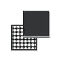
SPEAR320-2 STMicroelectronics, SPEAR320-2 Datasheet - Page 14

SPEAR320-2
Manufacturer Part Number
SPEAR320-2
Description
IC MPU ARM9 289LFBGA
Manufacturer
STMicroelectronics
Series
SPEAr®r
Datasheet
1.SPEAR320-2.pdf
(76 pages)
Specifications of SPEAR320-2
Processor Type
ARM Microprocessor
Speed
333MHz
Voltage
1.14 V ~ 3.6 V
Mounting Type
Surface Mount
Package / Case
289-LFBGA
Processor Series
SPEAr320
Core
ARM926EJ-S
Data Bus Width
16 bit
Maximum Clock Frequency
333 MHz
Operating Supply Voltage
1.2 V
Maximum Operating Temperature
+ 85 C
Mounting Style
SMD/SMT
Data Ram Size
8 KB
Interface Type
I2C, UART, USB, Serial
Number Of Programmable I/os
102
Number Of Timers
4
Program Memory Size
32 KB
Program Memory Type
ROM
Lead Free Status / RoHS Status
Lead free / RoHS Compliant
Features
-
Lead Free Status / Rohs Status
Lead free / RoHS Compliant
Other names
497-10843
Available stocks
Company
Part Number
Manufacturer
Quantity
Price
Architecture overview
3.7
3.8
3.9
14/76
Flexible static memory controller (FSMC)
SPEAr320 provides a Flexible Static Memory Controller (FSMC) which interfaces the AHB
bus to external parallel NAND Flash memories.
●
●
●
●
●
●
●
●
●
●
●
●
Multichannel DMA controller
Within its basic subsystem, SPEAr320 provides a DMA controller (DMAC) able to service up
to 8 independent DMA channels for serial data transfers between single source and
destination (i.e., memory-to-memory, memory-to-peripheral, peripheral to- memory, and
peripheral-to-peripheral).
Each DMA channel can support a unidirectional transfer, with internal four-word FIFO per
channel.
SMII/MII Ethernet controller
SPEAr320 features two Ethernet MACs, one supporting SMII and one supporting SMII and
MII.
Each MAC channel has dedicated TX/RX signals while synchronization and clock signals
are common for PHY connection.
Figure 3
Provides an interface between AHB system bus and external NAND Flash memory
devices.
8/16-bit wide data path
FSMC performs only one access at a time and only one external device is accessed
Supports little-endian and big-endian memory architectures
AHB burst transfer handling to reduce access time to external devices
Supplies an independent configuration for each memory bank
Programmable timings to support a wide range of devices
–
–
–
Independent chip select control for each memory bank
Shares the address bus and the data bus with all the external peripherals
Only chips selects are unique for each peripheral
External asynchronous wait control
Boot memory bank configurable at reset using external control pins
shows the typical SMII configuration:
Programmable wait states (up to 31)
Programmable bus turnaround cycles (up to 15)
Programmable output enable and write enable delays (up to 15)
Doc ID 16755 Rev 4
SPEAr320


