NHDev Development Board Newhaven Display, NHDev Development Board Datasheet - Page 6
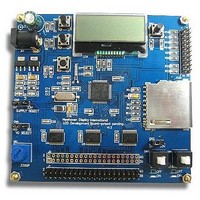
NHDev Development Board
Manufacturer Part Number
NHDev Development Board
Description
Display Modules & Development Tools LCD Development Brd 100 mm x 95 mm
Manufacturer
Newhaven Display
Datasheet
1.NHDEV.pdf
(12 pages)
Specifications of NHDev Development Board
Description/function
LCD Development Board
Interface Type
JTAG
Backlighting
No Backlighting
Data Bus Width
32 bit
Maximum Supply Current
600 mA
Module Size (w X H X T)
100 mm x 95 mm
Operating Current
600 mA
Operating Supply Voltage
7 V
Operating Voltage
7 V
Product
Display Modules
Software
Software Not Included
Touch Panel
No Touch Panel
For Use With/related Products
TFT, COG, Graphic, LCD Displays, Character
Lead Free Status / RoHS Status
Lead free / RoHS Compliant


Pins
CN2
CN4
CN3
13‐16
17‐20
21‐28
33‐36
37‐40
Pin
10
11
12
29
30
31
32
1
2
3
4
5
6
7
8
9
Output Pin Description
Jumper Pin Description
© 2 0 1 0 N e w h a v e n D i s p l a y I n t e r n a t i o n a l , I n c
SUPPLY SELECT
SUPPLY SELECT
BACKLIGHT
V0 SELECT
R/W or /WR
DB8 – DB15
DB0 – DB3
DB4 – DB7
SDI or SDA
SCK or SCL
Name
RS or A0
E or /RD
Symbol
or DISP
SPISS
/CS1
/CS2
/RES
VDD
VDD
VEE
VSS
BLE
BLE
VSS
V0
E2
5V / 3.3V Selectable 5V, 3.3V Logic Power Supply
5V / 3.3V
5V / 3.3V
5V / 3.3V
Variable
Level
Input
Level
GND
GND
3.3V
VDD
3.3V
VEE
H/L
H/L
H/L
H/L
H/L
H/L
H/L
H/L
H/L
H/L
H/L
H/L
H/L
5V
5V
Ground
LCD Contrast adjustment voltage selectable between VSS to VDD or VSS
to VEE
LCD voltage input (selected with J2)
Register Select. H=Instruction, L=Data
R/W in M6800 interface. H=Read, L=Write
/WR in I8080 interface. H=Write Inactive, L=Write Active
E in M6800 interface. H‐>L = Enable Strobe
/RD in I8080 interface. H=Read Inactive, L=Read Active
H‐> L = Enable Strobe for second controller
Chip Select. L=Chip Active
Chip Select‐Second Controller. L=Chip Active
DISP=Display ON signal
Reset. L=Reset controller.
Backlight power switch (SW5)
Bi‐directional 3‐state data bus lines. Not used in 4‐bit mode.
Bi‐directional 3‐state data bus lines.
Bi‐directional 3‐state data bus lines.
Serial Data In
Serial Clock
Serial Slave Select
Backlight power switch (SW5)
Selectable 5V, 3.3V Logic Power Supply
Ground
(pins 12,32)
logic pins
VDD and
Output
(pin 3)
SW5
V0
Select 5V as VDD for the display and logic
Select 3.3V as VDD for the display and logic
Select contrast voltage between VDD and VSS. (For a
Positive LCD voltage).
Adjustable via VR1 potentiometer.
Select contrast voltage between VSS and VEE. (For a
Negative LCD voltage).
VEE must be supplied externally onto PIN4.
Adjustable via VR1 potentiometer.
Select 5V as voltage supply for LED backlight.
External current limiting resistor may be required.
Select 3.3V as voltage supply for LED backlight.
External current limiting resistor may be required.
Description
Description
Rev. 9.7.10
P a g e
| 6
Related parts for NHDev Development Board
Image
Part Number
Description
Manufacturer
Datasheet
Request
R

Part Number:
Description:
DISPLAY VFD ALPHA 1X20 6.5MM
Manufacturer:
Newhaven Display
Datasheet:

Part Number:
Description:
DISPLAY VFD ALPHA 1X16 5MM
Manufacturer:
Newhaven Display
Datasheet:

Part Number:
Description:
DISPLAY VFD 7-SEG 1X9 9.7MM
Manufacturer:
Newhaven Display
Datasheet:

Part Number:
Description:
DISPLAY VFD 7-SEG 1X6 20MM
Manufacturer:
Newhaven Display
Datasheet:

Part Number:
Description:
DISPLAY VFD 7-SEG 1X19 11MM
Manufacturer:
Newhaven Display
Datasheet:

Part Number:
Description:
DISPLAY VFD 7-SEG 1X3 8MM
Manufacturer:
Newhaven Display
Datasheet:

Part Number:
Description:
DISPLAY VFD CUSTOM DVD
Manufacturer:
Newhaven Display
Datasheet:

Part Number:
Description:
DISPLAY VFD CUST AUDIO
Manufacturer:
Newhaven Display
Datasheet:

Part Number:
Description:
DISPLAY VFD CUST AUDIO
Manufacturer:
Newhaven Display
Datasheet:

Part Number:
Description:
DISPLAY VFD 7-SEG 1X5 7.6MM
Manufacturer:
Newhaven Display
Datasheet:

Part Number:
Description:
DISPLAY VFD CUST APPLIANCE
Manufacturer:
Newhaven Display
Datasheet:

Part Number:
Description:
DISPLAY VFD CUSTOM DVD
Manufacturer:
Newhaven Display
Datasheet:

Part Number:
Description:
DISPLAY VFD 7-SEG 1X4 7.6MM
Manufacturer:
Newhaven Display
Datasheet:

Part Number:
Description:
DISPLAY VFD 7-SEG 1X9 8MM
Manufacturer:
Newhaven Display
Datasheet:

Part Number:
Description:
DISPLAY VFD 7-SEG 1X7 12.5MM
Manufacturer:
Newhaven Display
Datasheet: