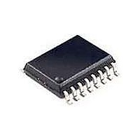
HV9961NG-G Supertex, HV9961NG-G Datasheet - Page 6

HV9961NG-G
Manufacturer Part Number
HV9961NG-G
Description
LED Drivers LED DRIVER WITH AVE RAGE-MODE (I) CNTRL
Manufacturer
Supertex
Datasheet
1.HV9961LG-G.pdf
(9 pages)
Specifications of HV9961NG-G
High Level Output Current
0.165 A
Operating Supply Voltage
8 V to 450 V
Maximum Power Dissipation
1000 mW
Maximum Operating Temperature
+ 125 C
Mounting Style
SMD/SMT
Package / Case
SOIC-16
Minimum Operating Temperature
- 40 C
Operating Supply Voltage (typ)
9/12/15/18/24V
Number Of Segments
1
Operating Temperature (min)
-40C
Operating Temperature (max)
125C
Operating Temperature Classification
Automotive
Package Type
SOIC N
Pin Count
16
Mounting
Surface Mount
Power Dissipation
1W
Lead Free Status / RoHS Status
Lead free / RoHS Compliant
Available stocks
Company
Part Number
Manufacturer
Quantity
Price
Company:
Part Number:
HV9961NG-G
Manufacturer:
Supertex
Quantity:
135
The short circuit protection comparator trips when the volt-
age at CS exceeds 0.44V. When this occurs, the GATE off-
time T
of the inductor current and potentially its saturation due to
insufficient output voltage. The typical short-circuit current is
shown in the waveform of Fig. 2.
A leading-edge blanking delay is provided at CS to prevent
false triggering of the current feedback and the short circuit
protection.
Linear Dimming
When the voltage at LD falls below 1.5V, the internal 275mV
reference to the constant-current feedback becomes over-
ridden by V
remains continuous, the LED current is given by the equa-
tion (3) above. However, when V
GATE output becomes disabled. The GATE signal recovers,
when V
tions to be able to shut the LED lamp off with the same signal
input that controls the brightness. The typical linear dimming
response is shown in Fig.3.
The linear dimming input could also be used for “mixed-
mode” dimming to expand the dimming ratio. In such case a
Fig.3. Typical linear dimming response of an HV9961
0.40
0.35
0.30
0.25
0.20
0.15
0.10
0.05
0.44V/R
HICCUP
0
LD
0
exceeds 200mV. This is required in some applica-
Fig.2. Short-circuit inductor current.
CS
LD
Supertex inc.
= 400µs is generated to prevent stair-casing
0.2
• 0.185. As long as the current in the inductor
LD Response Characteristics
0.4
400µs
LED driver
0.6
LD (V)
0.8
LD
●
falls below 150mV, the
1235 Bordeaux Drive, Sunnyvale, CA 94089
1.0
1.2
1.4
1.6
6
pulse-width modulated signal of a measured amplitude be-
low 1.5V should be applied at LD.
Input Voltage Regulator
The HV9961 can be powered directly from an 8.0 ~ 450VDC
supply through its VIN input. When this voltage is applied at
the VIN pin, the HV9961 maintains a constant 7.5V level at
VDD. This voltage can be used to power the IC and external
circuitry connected to VDD within the rated maximum cur-
rent or within the thermal ratings of the package, whichever
limit is lower. The VDD pin must be bypassed by a low ESR
capacitor to provide a low impedance path for the high fre-
quency current of the GATE output. The HV9961 can also be
powered through the VDD pin directly with a voltage greater
than the internally regulated 7.5V, but less than 12V.
Despite the instantaneous voltage rating of 450V, continu-
ous voltage at VIN is limited by the power dissipation in the
package. For example, when HV9961 draws I
from the VIN input, and the 8-pin SOIC package is used, the
maximum continuous voltage at VIN is limited to:
where the ambient temperature T
working junction temperature T
to-ambient thermal resistance R
In such cases, when it is needed to operate the HV9961
from a higher voltage, a resistor or a Zener diode can be
added in series with the VIN input to divert some of the
power loss from the HV9961. In the above example, using
a 100V Zener diode will allow the circuit to work up to 490V.
The input current drawn from the VIN pin is represented by
the following equation:
In the above equation, f
is the GATE charge of the external FET obtained from the
manufacturer’s datasheet.
GATE Output
The GATE output of the HV9961 is used to drive an external
MOSFET. It is recommended that the gate charge Q
external MOSFET be less than 25nC for switching frequen-
cies ≤100kHz and less than 15nC for switching frequencies
>100kHz.
V
I
IN
IN(MAX)
≈ 1.0mA + Q
●
Tel: 408-222-8888
=
(T
R
J(MAX)
θ,J-A
G
S
• f
is the switching frequency, and Q
• I
- T
S
IN
●
A
)
www.supertex.com
J(MAX)
θ,JA
= 390V
A
= 128
= 25
= 125
O
O
C, the maximum
C/W.
O
C, the junction-
HV9961
IN
= 2.0mA
G
of the
(5)
(6)
G


