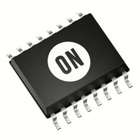
CAT4106YP-T2 ON Semiconductor, CAT4106YP-T2 Datasheet - Page 8

CAT4106YP-T2
Manufacturer Part Number
CAT4106YP-T2
Description
LED Drivers LED DRVR BOOST 4CH/10LED
Manufacturer
ON Semiconductor
Datasheet
1.CAT4106HV4-GT2.pdf
(15 pages)
Specifications of CAT4106YP-T2
Number Of Digits
4
Low Level Output Current
10 mA
High Level Output Current
175 mA
Operating Supply Voltage
- 0.3 V to 6 V
Maximum Supply Current
4.4 mA
Maximum Operating Temperature
+ 85 C
Mounting Style
SMD/SMT
Package / Case
TSSOP-16
Minimum Operating Temperature
- 40 C
Lead Free Status / RoHS Status
Lead free / RoHS Compliant
Available stocks
Company
Part Number
Manufacturer
Quantity
Price
Company:
Part Number:
CAT4106YP-T2
Manufacturer:
ON Semiconductor
Quantity:
1 978
Company:
Part Number:
CAT4106YP-T2
Manufacturer:
ON Semiconductor
Quantity:
950
Pin Descriptions
VIN is the supply pin for the device. The supply input
current needed for normal operation is approximately 2 mA
plus 3 times I
dimming, or whenever the converter is not switching, the
supply current will decrease by around 1 mA. The voltage
applied at VIN should be kept between 3 V and 5.5 V. A
small ceramic bypass capacitor of 0.1 mF or greater is
recommended to be in close proximity to the VIN pin.
EN/PWM is the device Enable and PWM dimming control
input for all LED channels. Guaranteed levels of logic high
and logic low are set at 1.3 V and 0.4 V respectively. During
normal PWM dimming, the entire device remains fully
biased and only the LED channels are pulsed on/off. The
device will only enter zero current shutdown mode after the
EN/PWM is help low for at least 5 ms typically. This pin has
an internal pull−down resistor of 200 kW.
RSET is the voltage regulated control pin for sensing the
desired programming current level to be applied on all LED
channels. During normal operation, the RSET pin is kept at
1.2 V and accurately monitors the current level in the
externally applied R1 resistor. The current transfer ratio
from RSET pin current to LED pin current is 100.
LED1 to LED4 provide the regulated current source for
driving each of the LED strings with a tightly matched
constant current. To ensure optimal performance, the bias
voltage on the LED channels should be set at a nominal
0.6 V or higher. Each channel is capable of driving a current
Table 5. PIN DESCRIPTION
EN/PWM
VFMAX
VFMIN
FAULT
PGND
Name
CTRL
RSET
LED1
LED4
LED3
LED2
GND
N.C.
TAB
SW
VIN
FB
RSET
pin current. During intervals of PWM
TSSOP−16
TQFN−16
TAB
10
11
12
13
14
15
16
1
2
3
4
5
6
7
8
9
LED1 cathode terminal
Signal Ground reference
Power Ground Reference (DC/DC Power Switch)
Feedback reference (300 mV) for setting LED channel operating voltage
Internal power FET switch drain connection
Device Enable (active high) and PWM control input
Not connected
Supply voltage for the device
LED channel operating voltage (lowest of all 4 channels)
Comparator input for setting the LED string short−circuit voltage limit
Comparator input for setting the LED string open−circuit voltage limit
RSET resistor pin for setting the LED channel operating current
LED4 cathode terminal
LED3 cathode terminal
LED2 cathode terminal
Thermal pad (connect to GND and PGND)
Open/Short LED Fault detection output (active−low)
http://onsemi.com
8
up to 175 mA. All channels immediately enter a high
impedance mode whenever the EN/PWM is taken LOW.
CTRL pin is a multiplexer output which selects the lowest
operating voltage appearing on any of the four LED output
drive channels. This control signal represents the cathode
terminal voltage of the LED string with greatest forward
voltage (V
can be used to set the lowest operating voltage of each
channel. External current loading of the CTRL pin is
recommended to be less than 25 mA.
FB is the voltage feedback control pin for the internal high
power DC/DC converter. This pin has a high impedance
input and its voltage remains accurately regulated to 0.3 V
during normal steady state operation.
SW pin is the drain terminal of the high voltage CMOS
power switch which has a typical on−resistance of 1 W and
is current limited to 1 A typically. An overvoltage protection
circuit places the device in a soft−clamping low power mode
if the voltage transients exceed 40 V.
VFMIN pin uses a pair of external resistors (R6 & R7) to
program the worst case, minimum LED string forward
voltage (V
during power−up, any LED string enters full regulation
before this programmed level is reached (VFMIN pin
voltage < 1.2 V), the string will be considered to contain
LEDs which are short−circuit and a fault condition will be
Function
F
FMIN
). An external resistor network from CTRL to FB
) expected in the specific application. If,


