HCPL2630 Fairchild Semiconductor, HCPL2630 Datasheet - Page 4
HCPL2630
Manufacturer Part Number
HCPL2630
Description
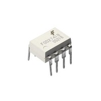
High Speed Optocouplers DIP-8 HS LOGIC GATE
Manufacturer
Fairchild Semiconductor
Datasheet
1.HCPL2630.pdf
(12 pages)
Specifications of HCPL2630
Isolation Voltage
2500 Vrms
Maximum Continuous Output Current
50 mA
Maximum Fall Time
0.012 us
Maximum Forward Diode Current
30 mA
Maximum Rise Time
75 ns
Output Device
Logic Gate Photo IC
Configuration
2 Channel
Maximum Baud Rate
10 Mbps
Maximum Forward Diode Voltage
1.75 V
Maximum Reverse Diode Voltage
5 V
Maximum Power Dissipation
60 mW
Maximum Operating Temperature
+ 85 C
Minimum Operating Temperature
- 40 C
Package / Case
DIP-8
No. Of Channels
2
Optocoupler Output Type
Logic Gate
Input Current
15mA
Output Voltage
7V
Opto Case Style
DIP
No. Of Pins
8
Input Current Max
15mA
Rohs Compliant
Yes
Lead Free Status / RoHS Status
Lead free / RoHS Compliant
Other names
HCPL2630_NL
Available stocks
Company
Part Number
Manufacturer
Quantity
Price
Company:

Part Number:
HCPL2630
Manufacturer:
AGILENT
Quantity:
5 530
Company:
Part Number:
HCPL2630
Manufacturer:
AGILENT
Quantity:
20 000
Part Number:
HCPL2630
Manufacturer:
HP
Quantity:
20 000
Part Number:
HCPL2630-000E
Manufacturer:
AVAGO/ه®‰هچژé«ک
Quantity:
20 000
Part Number:
HCPL2630-000E/HCPL-2630-000E
Manufacturer:
AVAGO/ه®‰هچژé«ک
Quantity:
20 000
Company:
Part Number:
HCPL2630020E
Manufacturer:
AVAGO
Quantity:
3 599
Part Number:
HCPL2630S
Manufacturer:
ON/ه®‰و£®ç¾ژ
Quantity:
20 000
Company:
Part Number:
HCPL2630SD
Manufacturer:
TI
Quantity:
2 200
Part Number:
HCPL2630SD
Manufacturer:
FAIRCHILD/ن»™ç«¥
Quantity:
20 000


©2005 Fairchild Semiconductor Corporation
6N137, HCPL2601, HCPL2611, HCPL2630, HCPL2631 Rev. 1.0.8
Electrical Characteristics
Transfer Characteristics
Isolation Characteristics
*All Typicals at V
Notes:
1. The V
2. Each channel.
3. Enable Input – No pull up resistor required as the device has an internal pull up resistor.
4. t
5. t
6. t
7. t
8. t
9. t
10. CM
11. CM
12. Device considered a two-terminal device: Pins 1, 2, 3 and 4 shorted together, and Pins 5, 6, 7 and 8 shorted
Symbol
Symbol
V
R
C
or solid tantalum capacitor with good high frequency characteristic and should be connected as close as possible
to the package V
pulse to the 1.5 V level on the LOW to HIGH transition of the output voltage pulse.
pulse to the 1.5 V level on the HIGH to LOW transition of the output voltage pulse.
voltage pulse to the 1.5V level on the LOW to HIGH transition of the output voltage pulse.
voltage pulse to the 1.5V level on the HIGH to LOW transition of the output voltage pulse.
HIGH state (i.e., V
LOW output state (i.e., V
together.
V
I
PLH
PHL
r
f
ELH
EHL
I
I
I-O
ISO
OH
– Rise time is measured from the 90% to the 10% levels on the LOW to HIGH transition of the output pulse.
– Fall time is measured from the 10% to the 90% levels on the HIGH to LOW transition of the output pulse.
FT
I-O
I-O
OL
L
H
– Propagation delay is measured from the 3.75mA level on the HIGH to LOW transition of the input current
– Propagation delay is measured from the 3.75mA level on the LOW to HIGH transition of the input current
– Enable input propagation delay is measured from the 1.5V level on the HIGH to LOW transition of the input
– Enable input propagation delay is measured from the 1.5V level on the LOW to HIGH transition of the input
– The maximum tolerable rate of rise of the common mode voltage to ensure the output will remain in the
– The maximum tolerable rate of rise of the common mode voltage to ensure the output will remain in the
CC
Input-Output Insulation
Leakage Current
Withstand Insulation Test
Voltage
Resistance (Input to Output)
Capacitance (Input to Output)
supply to each optoisolator must be bypassed by a 0.1µF capacitor or larger. This can be either a ceramic
HIGH Level Output Current
LOW Level Output Current
Input Threshold Current
CC
DC Characteristics
Characteristics
= 5V, T
CC
OUT
and GND pins of each device.
> 2.0V). Measured in volts per microsecond (V/µs).
A
= 25°C
OUT
(T
(T
A
A
< 0.8V). Measured in volts per microsecond (V/µs).
= -40 to +85°C unless otherwise specified)
= -40°C to +85°C unless otherwise specified.)
(Continued)
V
I
V
I
V
I
F
CL
OL
Relative humidity = 45%,
T
V
RH < 50%, T
I
V
f = 1MHz
I-O
CC
CC
CC
A
I-O
I-O
= 250µA, V
= 13mA
= 25°C, t = 5s,
= 13mA
Test Conditions
≤ 2µA, t = 1 min.
= 5.5V, V
= 5.5V, I
= 5.5V, V
= 3000 VDC
= 500V
Test Conditions
(12)
(2)
(12)
F
A
E
O
O
4
= 5mA, V
= 25°C,
= 2.0V
= 5.5V,
= 0.6V, V
(12)
(12)
(2)
E
E
= 2.0V,
= 2.0V,
Min.
2500
Min.
Typ.*
10
0.6
12
Typ.*
.35
3
Max.
1.0*
Max.
100
0.6
5
www.fairchildsemi.com
V
Unit
Unit
µA
pF
RMS
mA
Ω
µA
V
Related parts for HCPL2630
Image
Part Number
Description
Manufacturer
Datasheet
Request
R

Part Number:
Description:
Fairchild Semiconductor [IGBT MODULE]
Manufacturer:
Fairchild Semiconductor
Datasheet:

Part Number:
Description:
Discrete Semiconductor Modules
Manufacturer:
Fairchild Semiconductor
Part Number:
Description:
Discrete Semiconductor Modules
Manufacturer:
Fairchild Semiconductor
Part Number:
Description:
This N-Channel MOSFET is produced using Fairchild Semiconductor’s advanced Power Trench® process
Manufacturer:
Fairchild Semiconductor
Datasheet:
Part Number:
Description:
This N-Channel MOSFET is produced using Fairchild Semiconductor’s advanced Power Trench® process
Manufacturer:
Fairchild Semiconductor
Datasheet:
Part Number:
Description:
This N-Channel MOSFET is produced using Fairchild Semiconductor’s advanced PowerTrench® process
Manufacturer:
Fairchild Semiconductor
Datasheet:
Part Number:
Description:
This N-Channel MOSFET is produced using Fairchild Semiconductor’s advanced PowerTrench® process
Manufacturer:
Fairchild Semiconductor
Datasheet:
Part Number:
Description:
This N-Channel MOSFET is produced using Fairchild Semiconductor’s advanced Power Trench® process
Manufacturer:
Fairchild Semiconductor
Datasheet:
Part Number:
Description:
This N-Channel logic Level MOSFETs are produced using Fairchild Semiconductor‘s advanced Power Trench® process that has been special tailored to minimize the on-state resistance and yet maintain superior switching performance
Manufacturer:
Fairchild Semiconductor
Datasheet:
Part Number:
Description:
This N-Channel MOSFET is produced using Fairchild Semiconductor’s advanced Power Trench® process
Manufacturer:
Fairchild Semiconductor
Datasheet:
Part Number:
Description:
This N-Channel SyncFET™ is produced using Fairchild Semiconductor’s advanced PowerTrench® process
Manufacturer:
Fairchild Semiconductor
Datasheet:
Part Number:
Description:
This N-Channel SyncFET™ is produced using Fairchild Semiconductor’s advanced PowerTrench® process
Manufacturer:
Fairchild Semiconductor
Datasheet:
Part Number:
Description:
This N-Channel SyncFET™ is produced using Fairchild Semiconductor’s advanced PowerTrench® process
Manufacturer:
Fairchild Semiconductor
Datasheet:
Part Number:
Description:
This N-Channel logic Level MOSFETs are produced using Fairchild Semiconductor‘s advanced Power Trench® process that has been special tailored to minimize the on-state resistance and yet maintain superior switching performance
Manufacturer:
Fairchild Semiconductor
Datasheet:
Part Number:
Description:
This N-Channel MOSFET is produced using Fairchild Semiconductor’s advanced Power Trench® process that has been especially tailored to minimize the on-state resistance and yet maintain superior switching performance
Manufacturer:
Fairchild Semiconductor
Datasheet: