TCET1100G Vishay, TCET1100G Datasheet - Page 3
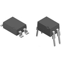
TCET1100G
Manufacturer Part Number
TCET1100G
Description
Transistor Output Optocouplers Phototransistor Out Single CTR 50-600%
Manufacturer
Vishay
Specifications of TCET1100G
Isolation Voltage
5000 Vrms
Maximum Input Diode Current
60 mA
Maximum Reverse Diode Voltage
6 V
Output Device
Transistor
Output Type
DC
Configuration
1
Input Type
DC
Maximum Collector Emitter Voltage
70 V
Maximum Collector Emitter Saturation Voltage
300 mV
Current Transfer Ratio
600 %
Maximum Forward Diode Voltage
1.6 V
Maximum Collector Current
50 mA
Maximum Power Dissipation
265 mW
Maximum Operating Temperature
+ 100 C
Minimum Operating Temperature
- 40 C
Package / Case
PDIP-4
No. Of Channels
1
Optocoupler Output Type
Phototransistor
Input Current
50mA
Output Voltage
70V
Opto Case Style
DIP
No. Of Pins
4
Mounting Type
Through Hole
Approval Bodies
VDE, CSA, BSI EN
Rohs Compliant
Yes
Lead Free Status / RoHS Status
Lead free / RoHS Compliant
Lead Free Status / RoHS Status
Lead free / RoHS Compliant, Lead free / RoHS Compliant
Available stocks
Company
Part Number
Manufacturer
Quantity
Price

Part Number:
TCET1100G
Manufacturer:
VISHAY/威世
Quantity:
20 000


Coupler
Thermal Characteristics
The thermal model is represented in the thermal network below. Each resistance value given in this model can be used to calculate the tem-
peratures at each node for a given operating condition. The thermal resistance from board to ambient will be dependent on the type of PCB,
layout and thickness of copper traces. For a detailed explanation of the thermal model, please reference Vishay's Thermal Characteristics
of Optocouplers Application note.
* For 2 layer FR4 board (4" x 3" x 0.062)
Document Number 83503
Rev. 2.2, 05-Sep-06
Isolation test voltage (RMS)
Operating ambient temperature
range
Storage temperature range
Soldering temperature
LED Power dissipation
Output Power dissipation
Maximum LED junction temperature
Maximum output die junction temperature
Thermal resistance, Junction Emitter to Board
Thermal resistance, Junction Emitter to Case
Thermal resistance, Junction Detector to Board
Thermal resistance, Junction Detector to Case
Thermal resistance, Junction Emitter to Junction Detector
Thermal resistance, Board to Ambient*
Thermal resistance, Case to Ambient*
Parameter
T
19996
JD
θ
DB
Parameter
θ
DC
t = 1 min
2 mm from case t ≤ 10 s
T
T
T
B
C
A
θ
DE
T
θ
θ
A
Test condition
CA
BA
θ
Package
EC
θ
EB
T
JE
at 25 °C
at 25 °C
Test condition
Symbol
TCET1100/TCET1100G
T
V
T
T
amb
ISO
stg
sld
- 40 to + 100
- 55 to + 125
Symbol
Vishay Semiconductors
Value
T
T
5000
P
P
θ
θ
θ
θ
θ
θ
θ
260
jmax
jmax
diss
diss
EC
DB
DC
ED
CA
EB
BA
Value
4041
100
150
125
125
173
149
111
127
173
197
www.vishay.com
V
Unit
RMS
°C
°C
°C
°C/W
°C/W
°C/W
°C/W
°C/W
°C/W
°C/W
Unit
mW
mW
°C
°C
3
Related parts for TCET1100G
Image
Part Number
Description
Manufacturer
Datasheet
Request
R

Part Number:
Description:
357-036-542-201 CARDEDGE 36POS DL .156 BLK LOPRO
Manufacturer:
Vishay
Datasheet:
Part Number:
Description:
357-036-542-201 CARDEDGE 36POS DL .156 BLK LOPRO
Manufacturer:
Vishay
Datasheet:
Part Number:
Description:
357-036-542-201 CARDEDGE 36POS DL .156 BLK LOPRO
Manufacturer:
Vishay
Datasheet:
Part Number:
Description:
357-036-542-201 CARDEDGE 36POS DL .156 BLK LOPRO
Manufacturer:
Vishay
Datasheet:
Part Number:
Description:
357-036-542-201 CARDEDGE 36POS DL .156 BLK LOPRO
Manufacturer:
Vishay
Datasheet:
Part Number:
Description:
357-036-542-201 CARDEDGE 36POS DL .156 BLK LOPRO
Manufacturer:
Vishay
Datasheet:
Part Number:
Description:
357-036-542-201 CARDEDGE 36POS DL .156 BLK LOPRO
Manufacturer:
Vishay
Datasheet:
Part Number:
Description:
357-036-542-201 CARDEDGE 36POS DL .156 BLK LOPRO
Manufacturer:
Vishay
Datasheet:
Part Number:
Description:
357-036-542-201 CARDEDGE 36POS DL .156 BLK LOPRO
Manufacturer:
Vishay
Datasheet:
Part Number:
Description:
357-036-542-201 CARDEDGE 36POS DL .156 BLK LOPRO
Manufacturer:
Vishay
Datasheet:
Part Number:
Description:
357-036-542-201 CARDEDGE 36POS DL .156 BLK LOPRO
Manufacturer:
Vishay
Datasheet:
Part Number:
Description:
357-036-542-201 CARDEDGE 36POS DL .156 BLK LOPRO
Manufacturer:
Vishay
Datasheet:
Part Number:
Description:
357-036-542-201 CARDEDGE 36POS DL .156 BLK LOPRO
Manufacturer:
Vishay
Datasheet:
Part Number:
Description:
357-036-542-201 CARDEDGE 36POS DL .156 BLK LOPRO
Manufacturer:
Vishay
Datasheet:
Part Number:
Description:
357-036-542-201 CARDEDGE 36POS DL .156 BLK LOPRO
Manufacturer:
Vishay
Datasheet: